News Posts matching #7 nm

Return to Keyword Browsing

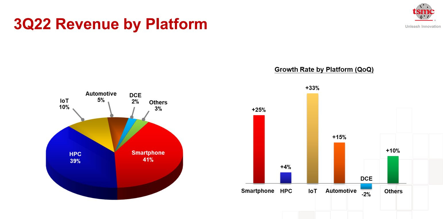
Top 10 TSMC Customers Said to have Cut Orders for 2023

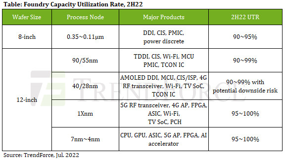
On the day of TSMC's celebration of the mass production start of its 3 nm node, news out of Taiwan suggests that all of its top 10 customers have cut their orders for 2023. However, the cuts are unlikely to affect its new node, but rather its existing nodes, with the 7 and 6 nm nodes said to be hit the hardest, by as much as a 50 percent utilisation reduction in the first quarter of 2023. The 28 nm and 5 and 4 nm nodes are also said to be affected, although it's unclear by how much at this point in time.

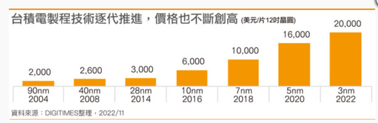
Revenue is expected to fall by at least 15 percent in the first quarter of 2023 for TSMC, based on numbers from DigiTimes. The fact that TSMC has increased its 2023 pricing by six percent should at least help offset some of the potential losses for the company, but it all depends on the demand for the rest of the year. Demand for mobile devices is down globally, which is part of the reason why so many of TSMC's customers have cut back their orders, as Apple, Qualcomm and Mediatek all produce their mobile SoCs at TSMC. Add to this that the demand for computers and new computer components are also down, largely due to the current pricing and TSMC is in for a tough time next year.

Huawei Prepares EUV Scanner for Sub-7 nm Chinese Chips

Huawei, the Chinese technology giant, has reportedly filed patents that it is developing extreme ultraviolet (EUV) scanners for use in the manufacturing process of semiconductors. This news comes amid increasing tensions between Huawei and the US government, which has imposed a series of sanctions on the company in recent years. According to UDN, Huawei has filed a patent that covers the entire EUV scanner with a 13.5 nm EUV light source, mirrors, lithography for printing circuits, and proper system control. While filing a patent is not the same as creating an accurate EUV scanner, it could enable China to produce a class of chips below 7 nm and have a homegrown semiconductor production, despite the ever-increasing US sanctions.

The development of EUV scanners is a significant milestone for Huawei and the semiconductor industry. However, the company's progress in this area may be hindered by the US government's sanctions, which have limited Huawei's access to certain technologies and markets. It is important to note that Chinese SMIC wanted to develop EUV fabrication based on third-party EUV tools; however, those plans were scrapped as the Wassenaar agreement came into action and prohibited the sales of advanced tools to Chinese companies. Huawei's development could represent a new milestone for the entire Chinese industry.

Achronix Announces Speedster7t AC7t1500 FPGA General Availability

In a continuing commitment to enabling industry-leading data acceleration in heterogeneous compute environments, Achronix Semiconductor Corporation, the industry's only independent supplier of high-end FPGAs and eFPGA IP solutions, today announced the production release of its AC7t1500 FPGA and the addition of the power-efficient AC7t800 FPGA to the Achronix Tool Suite.

"The Speedster 7t product family offers unprecedented FPGA-based performance for data acceleration applications," said Steve Mensor, VP of Marketing and Business Development at Achronix. "The release of the AC7t1500 to production along with the addition of the AC7t800 in our ACE design tools gives customers multiple options from this industry-leading, high-performance family that offers FPGA programmability with ASIC-level performance. These advancements give customers confidence that they can design on a robust, validated FPGA product family that meets their high-performance and high-bandwidth needs."

Global Top 10 Foundries' Total Revenue Grew by 6% QoQ for 3Q22, but Foundry Industry's Revenue Performance Will Enter Correction Period in 4Q22

According to TrendForce's research, the total revenue of the global top 10 foundries rose by 6% QoQ to US$35.21 billion for 3Q22 as the release of the new iPhone series during the second half of the year generated significant stock-up activities across Apple's supply chain. However, the global economy shows weak performances, and factors such as China's policy on containing COVID-19 outbreaks and high inflation continue to impact consumer confidence. As a result, peak-season demand in the second half of the year has been underwhelming, and inventory consumption is proceeding slower than anticipated. This situation has led to substantial downward corrections to foundry orders as well. For 4Q22, TrendForce forecasts that the total revenue of the global top 10 foundries will register a QoQ decline, thereby terminating the boom of the past two years—when there was an uninterrupted trend of QoQ revenue growth.

Regarding individual foundries' performances in 3Q22, the group of the top five was led by TSMC, followed by Samsung, UMC, GlobalFoundries, and SMIC. Their collective global market share (in revenue terms) came to 89.6%. Most foundries were directly impacted by clients slowing down their stock-up activities or significantly correcting down their orders. Only TSMC was able to make a notable gain due to Apple's strong stock-up demand for the SoCs deployed in this year's new iPhone models. TSMC saw its revenue rise by 11.1% QoQ to US$20.16 billion, and the corresponding market share expanded to 56.1%. The growth was mainly attributed to the ≤7 nm nodes, whose share in the foundry's revenue had kept climbing and reached 54% in the third quarter. Conversely, Samsung actually experienced a slight QoQ drop of 0.1% in foundry revenue even though it had also benefited from the component demand related to the new iPhone series. Partially impacted by the weakening of the Korean won, Samsung's market share fell to 15.5%.

AMD to Increase Xilinx FPGA Prices by up to 25%

Xilinx Field Programmable Gate Arrays (FPGAs), now part of AMD, are always in demand in the semiconductor industry. Today, AMD has shared a letter to Xilinx customers that the selected FPGA device series will receive an 8-25% price increase. Citing AMD's investment into the supply chain, along with increased prices from the suppliers, Xilinx FPGAs will get more expensive. From January 9, 2023, the cost of the Spartan 6 series will increase by 25%, the price of the Versal series will not increase, and all other Xilinx products will increase by 8%. Interestingly, the older series manufactured on 40-28 nm nodes will increase while the latest Versal series doesn't experience any change.

Regarding lead times, the 16 nm UltraScale+ series, 20 nm UltraScale series, and 28 nm 7 series all take 20 weeks from order to delivery, which will remain until the third quarter of 2023. You can read the entire document below.

TSMC 3 nm Wafer Pricing to Reach $20,000; Next-Gen CPUs/GPUs to be More Expensive

Semiconductor manufacturing is a significant investment that requires long lead times and constant improvement. According to the latest DigiTimes report, the pricing of a 3 nm wafer is expected to reach $20,000, which is a 25% increase in price over a 5 nm wafer. For 7 nm, TSMC managed to produce it for "just" $10,000; for 5 nm, it costs the company to make it for the $16,000 mark. And finally, the latest and greatest technology will get an even higher price point at $20,000, a new record in wafer pricing. Since TSMC has a proven track record of delivering constant innovation, clients are expected to remain on the latest tech purchasing spree.

Companies like Apple, AMD, and NVIDIA are known for securing orders for the latest semiconductor manufacturing node capacities. With a 25% increase in wafer pricing, we can expect the next-generation hardware to be even more expensive. Chip manufacturing price is a significant price-determining factor for many products, so the 3 nm edition of CPUs, GPUs, etc., will get the highest difference.

AMD Explains the Economics Behind Chiplets for GPUs

AMD, in its technical presentation for the new Radeon RX 7900 series "Navi 31" GPU, gave us an elaborate explanation on why it had to take the chiplets route for high-end GPUs, devices that are far more complex than CPUs. The company also enlightened us on what sets chiplet-based packages apart from classic multi-chip modules (MCMs). An MCM is a package that consists of multiple independent devices sharing a fiberglass substrate.

An example of an MCM would be a mobile Intel Core processor, in which the CPU die and the PCH die share a substrate. Here, the CPU and the PCH are independent pieces of silicon that can otherwise exist on their own packages (as they do on the desktop platform), but have been paired together on a single substrate to minimize PCB footprint, which is precious on a mobile platform. A chiplet-based device is one where a substrate is made up of multiple dies that cannot otherwise independently exist on their own packages without an impact on inter-die bandwidth or latency. They are essentially what should have been components on a monolithic die, but disintegrated into separate dies built on different semiconductor foundry nodes, with a purely cost-driven motive.

Andes Technology Unveils The AndesCore AX60 Series, An Out-Of-Order Superscalar Multicore RISC-V Processor Family

Today, at Linley Fall Processor Conference 2022, Andes Technology, a leading provider of high efficiency, low power 32/64-bit RISC-V processor cores and founding premier member of RISC-V International, reveals its top-of-the-line AndesCore AX60 series of power and area efficient out-of-order 64-bit processors. The family of processors are intended to run heavy-duty OS and applications with compute intensive requirements such as advanced driver-assistance systems (ADAS), artificial intelligence (AI), augmented/virtual reality (AR/VR), datacenter accelerators, 5G infrastructure, high-speed networking, and enterprise storage.

The first member of the AX60 series, the AX65, supports the latest RISC-V architecture extensions such as the scalar cryptography extension and bit manipulation extension. It is a 4-way superscalar with Out-of-Order (OoO) execution in a 13-stage pipeline. It fetches 4 to 8 instructions per cycle guided by highly accurate TAGE branch predictor with loop prediction to ensure fetch efficiency. It then decodes, renames and dispatches up to 4 instructions into 8 execution units, including 4 integer units, 2 full load/store units, and 2 floating-point units. Besides the load/store units, the AX65's aggressive memory subsystem also includes split 2-level TLBs with multiple concurrent table walkers and up to 64 outstanding load/store instructions.

TSMC Cuts Back CAPEX Budget Despite Record Profits

Another quarter, another record breaking earnings report by TSMC, but it seems like the company has released that things are set to slow down sooner than initially expected and the company is hitting the brakes on some of its expansion projects. The company saw a 79.7 percent increase in profits compared to last year, with a profit of US$8.8 billion and a revenue of somewhere between US$19.9 to US$ 20.7 billion for the third quarter, which is a 47.9 percent bump compared to last year. TSMC's 5 nm nodes were the source for 28 percent of the revenues, followed by 26 percent for 7 nm nodes, 12 percent for 16 nm and 10 percent for 28 nm, with remaining nodes at 40 nm and larger making up for the remainder of the revenue. By platform, smartphone chips made up 41 percent, followed by High Performance Computing at 39 percent, IoT at 10 percent and automotive at five percent.

TSMC said it will cut back its CAPEX budget by around US$4 billion, to US$36 billion, compared to the earlier stated US$40 billion budget the company had set aside for expanding its fabs. Part of the reason for this is that TSMC is already seeing weaker demand for products manufactured using its N7 and N6 nodes, as the N7 node was meant to be a key part of the new fab in Kaohsiung in southern Taiwan. TSMC is expecting to start production on its first N3 node later this quarter and is expecting the capacity to be fully utilised for all of 2023. Supply is said to be exceeding demand, which TSMC said is partially to blame on tooling delivery issues. TSMC is expecting next year's revenue for its N3 node to be higher than its N5 node in 2020, although the revenue is said to be in the single digit percentage range. The N3E node is said to start production sometime in the second half of next year, or about a quarter earlier than expected. The N2 node isn't due to start production until 2025, but TSMC is already having very high customer engagement, so it doesn't look like TSMC is likely to suffer from a lack of business in the foreseeable future, as long as the company keeps delivering new nodes as planned.

US Strengthens China Export Bans, Limiting Access to Manufacturing Technology

The US Department of Commerce is in the process of increasing the stranglehold in tech exports directed to Chinese shores. The move is being made through the delivery of letters to US-based technology companies - namely KLA Corp, Lam Research Corp and Applied Materials Inc. - ordering them to stop the export of machines and equipment that can be used for sub-14 nm manufacturing. The move by the Department of Commerce only has validity for the companies that have been served by such a letter - at least until the Department codifies its newest regulations.

This means that only sellers with approved export licenses can keep doing business with Beijing, thus limiting the US companies China can work with as it aims to achieve at least a degree of self-sufficiency in the latest chipmaking tech. Perhaps the decision has come too late, however, as China's mainstay silicon manufacturing, SMIC, already manufactures chips at the 14 nm process (chips that have been deployed in China's Tinahu Light supercomputer already) and has even showcased manufacturing capability in the 7 nm field. It pays to remember that the US already had applied similar restrictions on equipment experts to China for the better part of two years - which apparently did little to stem China's capability to create increasingly denser semiconductor designs.

BIREN BR100 Detailed: China's AI-HPC Processor Storms into the HPC GPU Big Leagues

If InnoSilicon's Fenghua gaming GPU hit the scene last November seemingly out of nowhere, then another Chinese GPU developer is making waves at HotChips 22, this time in the enterprise space. The BR100 by BIREN is a large AI-HPC GPU-based processor that's China's answer to the Hopper, Ponte Vecchio, and CDNA2, and ensure China's growth as an AI/HPC leader is unaffected in the event of a tech embargo for whatever reason.

The BR100 is an MCM of two planar-silicon dies built on the 7 nm DUV node, with a striking 77 billion transistor-count between them, and 550 W TDP (typical). The chip features 64 GB of on-package HBM2E memory. System bus interfaces include PCI-Express 5.0 x16 with CXL, and eight lanes of a proprietary interconnect called B-Link, which total 2.3 TB/s of bandwidth. The processor supports nearly all popular compute formats except double-precision floating-point, or FP64. Among the supported ones are single-precision or FP32, TF32+, FP16, BF16, INT16, and INT8. BIREN claims up to 256 TFLOP/s FP32, up to 512 TFLOP/s TF32+, up to 1 PFLOP/s BF16, and 2,048 TOPS INT8. This would put it at 2.4 to 2.8 times faster than NVIDIA's "Ampere" A100.

AMD Readies a Handful New Ryzen PRO 5000 Desktop Processor SKUs

AMD is readying a handful new Ryzen PRO 5000 series desktop processor models, according to a leaked Lenovo datasheet for commercial desktops. These Socket AM4 processors are based on either the 7 nm "Renoir" monolithic silicon with "Zen 2" CPU cores; or the "Vermeer" MCM with "Zen 3" cores; all feature 65 W TDP, and the AMD PRO feature-set that rivals Intel vPro, including a framework for remote management, AMD PRO Security, PRO Manageability, and PRO Business (a priority tech-support channel).

Models in the lineup include the Ryzen 3 PRO 4350G, a "Renoir" based APU with a 4-core/8-thread "Zen 2" CPU clocked up to 4.00 GHz, and Radeon Vega 6 integrated graphics. The Ryzen 5 PRO 5645 is based on "Vermeer," and is a 6-core/12-thread "Zen 3" processor with 32 MB of L3 cache, and up to 4.60 GHz clock speeds. The Ryzen 7 PRO 5845 is the 8-core/16-thread model in the lineup, clocked up to 4.60 GHz. Leading the pack is the Ryzen 9 5945, a 12-core/24-thread chip clocked up to 4.70 GHz. From the looks of it, these processors will be exclusively available in the OEM channel, but AMD's OEM-only chips inevitably end up in the retail channel where they're sold loose from trays.

Chinese SMIC Ships 7 nm Chips, Reportedly Copied TSMC's Design

The Chinese technology giant, SMIC, has managed to advance its semiconductor manufacturing technology and shipped the first 7 nm silicon manufactured on China's soil. According to analyst firm TechInsights, who examined the 7 nm Bitcoin mining SoC made for MinerVa firm, there are doubts that SMIC 7 nm process is somewhat similar to TSMC's 7 nm process. Despite having no access to advanced semiconductor manufacturing tools, and US restrictions placed around it, SMIC has managed to produce what resembles an almost perfect 7 nm node. This could lead to a true 7 nm logic and memory bitcells sometimes in the future, as the node advances in SMIC's labs.

Having done an in-depth die analysis, the TechInsights report indicates that TSMC, Intel, and Samsung have a more advanced 7 nm node and are two nodes ahead of the Chinese SMIC. The results are not great regarding the economics and yield of this SMIC 7 nm process. While we have no specific data, the report indicates that the actual working chips made with older DUV tools are not perfect. This is not a problem for the Chinese market as it seeks independence from Western companies and technology. However, introducing a China-made 7 nm chip is more critical as it shows that the country can manufacture advanced nodes with restrictions and sanctions in place. The MinerVa SoC die and the PCB that houses those chips are pictured below.

TSMC Reports Second Quarter EPS of NT$9.14

TSMC (TWSE: 2330, NYSE: TSM) today announced consolidated revenue of NT$534.14 billion, net income of NT$237.03 billion, and diluted earnings per share of NT$9.14 (US$1.55 per ADR unit) for the second quarter ended June 30, 2022. Year-over-year, second quarter revenue increased 43.5% while net income and diluted EPS both increased 76.4%. Compared to first quarter 2022, second quarter results represented an 8.8% increase in revenue and a 16.9% increase in net income. All figures were prepared in accordance with TIFRS on a consolidated basis.

In US dollars, second quarter revenue was $18.16 billion, which increased 36.6% year-over-year and increased 3.4% from the previous quarter. Gross margin for the quarter was 59.1%, operating margin was 49.1%, and net profit margin was 44.4%. In the second quarter, shipments of 5-nanometer accounted for 21% of total wafer revenue; 7- nanometer accounted for 30%. Advanced technologies, defined as 7-nanometer and more advanced technologies, accounted for 51% of total wafer revenue.

Semiconductor Fab Order Cancellations Expected to Result in Reduced Capacity Utilization Rate in 2H22

According to TrendForce investigations, foundries have seen a wave of order cancellations with the first of these revisions originating from large-size Driver IC and TDDI, which rely on mainstream 0.1X μm and 55 nm processes, respectively. Although products such as MCU and PMIC were previously in short supply, foundries' capacity utilization rate remained roughly at full capacity through their adjustment of product mix. However, a recent wave cancellations have emerged for PMIC, CIS, and certain MCU and SoC orders. Although still dominated by consumer applications, foundries are beginning to feel the strain of the copious order cancellations from customers and capacity utilization rate has officially declined.

Looking at trends in 2H22, TrendForce indicates, in addition to no relief from the sustained downgrade of driver IC demand, inventory adjustment has begun for smartphones, PCs, and TV-related peripheral components such as SoCs, CIS, and PMICs, and companies are beginning to curtail their wafer input plans with foundries. This phenomenon of order cancellations is occurring simultaneously in 8-inch and 12-inch fabs at nodes including 0.1X μm, 90/55 nm, and 40/28 nm. Not even the advanced 7/6 nm processes are immune.

Intel 4 Process Node Detailed, Doubling Density with 20% Higher Performance

Intel's semiconductors nodes have been quite controversial with the arrival of the 10 nm design. Years in the making, the node got delayed multiple times, and only recently did the general public get the first 10 nm chips. Today, at IEEE's annual VLSI Symposium, we get more details about Intel's upcoming nodes, called Intel 4. Previously referred to as a 7 nm process, Intel 4 is the company's first node to use EUV lithography accompanied by various technologies. The first thing when a new process node is discussed is density. Compared to Intel 7, Intel 4 will double the transistor count for the same area and enable 20% higher performing transistors.

Looking at individual transistor size, the new Intel 4 node represents a very tiny piece of silicon that is even smaller than its predecessor. With a Fin Pitch of 30 nm, Contact Gate Poly Pitch of 50 nm between gates, and Minimum Metal Pitch (M0) of 50 nm, the Intel 4 transistor is significantly smaller compared to the Intel 7 cell, listed in the table below. For scaling, Intel 4 provides double the number of transistors in the same area compared to Intel 7. However, this reasoning is applied only to logic. For SRAM, the new PDK provides 0.77 area reduction, meaning that the same SoC built on Intel 7 will not be half the size of Intel 4, as SRAM plays a significant role in chip design. The Intel 7 HP library can put 80 million transistors on a square millimeter, while Intel 4 HP is capable of 160 million transistors per square millimeter.

Sapphire Radeon 6700 Graphics Cards Real: No RX, No XT

Sapphire formally launched its Radeon 6700 series graphics card. The AMD Radeon 6700 is an odd-ball SKU that doesn't yet feature in the company's retail product stack, but is yet being released to retail by Sapphire. So far we've not come across any other board partner with this SKU. The 6700 is unique in its branding—there's neither "RX" nor "XT" in the model name, it's called simply the "Radeon 6700."

Carved out from the same 7 nm "Navi 22" silicon as the RX 6700 XT and RX 6750 XT; the 6700 has 36 out of 40 compute units enabled, working out to 2,304 stream processors, and 144 TMUs. The card is endowed with 10 GB of 16 Gbps GDDR6 memory across a 160-bit wide memory interface. Sapphire has two cards in its lineup, one is an unnamed base model that sticks to the "reference" specs, and a factory-overclocked Pulse 6700 card.

Habana Labs Launches Second-generation AI Deep Learning Processors

Today at the Intel Vision conference, Habana Labs, an Intel company, announced its second-generation deep learning processors, the Habana Gaudi 2 Training and Habana Greco Inference processors. The processors are purpose-built for AI deep learning applications, implemented in 7nm technology and build upon Habana's high-efficiency architecture to provide customers with higher-performance model training and inferencing for computer vision and natural language applications in the data center. At Intel Vision, Habana Labs revealed Gaudi2's training throughput performance for the ResNet-50 computer vision model and the BERT natural language processing model delivers twice the training throughput over the Nvidia A100-80GB GPU.

"The launch of Habana's new deep learning processors is a prime example of Intel executing on its AI strategy to give customers a wide array of solution choices - from cloud to edge - addressing the growing number and complex nature of AI workloads. Gaudi2 can help Intel customers train increasingly large and complex deep learning workloads with speed and efficiency, and we're anticipating the inference efficiencies that Greco will bring."—Sandra Rivera, Intel executive vice president and general manager of the Datacenter and AI Group

AMD Announces Ryzen 5000C "Zen 3" Processors for Chromebooks

AMD today announced the Ryzen 5000C line of mobile processors for Chromebooks. This is the company's second generation of Chromebook-specific processors after the Ryzen 3000C series based on the original "Zen" microarchitecture. The 5000C series chips are based on "Zen 3," with CPU core counts of up to 8-core, and hence present a big leap in performance over the 3000C series, along with a complete suite of the latest connectivity, display technology, and security and management features specific to Chrome OS.

The Ryzen 5000C series is based on the 7 nm "Cezanne" monolithic silicon. The chip physically features an 8-core/16-thread CPU based on the "Zen 3" microarchitecture, with 16 MB of shared L3 cache; an iGPU based on the Vega graphics architecture, with 8 compute units (512 stream processors), a dual-channel DDR4 or LPDDR4/x memory interface, and unlike the conventional Ryzen 5000-series mobile processors, these chips come with a special microcode to match the security and management features of Chrome OS. AMD also supplies Chromebook vendors with timely driver updates for the various components on these chips.

PowerColor Radeon RX 6650 XT Hellhound Specs Sheet Hints at Clock Speed Increases Over RX 6600 XT

A leaked specifications sheet of the upcoming PowerColor Radeon RX 6650 XT Hellhound custom-design graphics card, seen by VideoCards, sheds light on AMD's play at carving out the RX 6650 XT. It involves dialing up the engine clocks (GPU clock speed), and memory bandwidth. At this point it is not known if the RX 6650 XT is based on a refined variant of the "Navi 23" silicon, possibly leveraging the TSMC N6 (6 nm) process, or if it's just a case of AMD dialing up clock speeds while pushing up the typical board power, on existing 7 nm (TSMC N7) process.

The RX 6650 XT Hellhound comes with about 4.3% increase in game clocks in its default "OC mode" BIOS, and about 3.7% increase in maximum boost clocks, up from 2593 MHz to 2689 MHz. The "Silent mode" BIOS of the RX 6650 XT Hellhound offers better clock speeds than the "OC mode" BIOS of the RX 6600 XT Hellhound, at 2410 MHz game, 2635 MHz boost, compared to 2382 MHz game, 2593 MHz boost. The other big surprise is memory clocks, with AMD possibly using 17.5 Gbps GDDR6 memory speeds, compared to 16 Gbps on the RX 6600 XT. This results in a 9.4% increase in memory bandwidth. The RX 6600 XT Hellhound uses a single 8-pin PCIe power connector, for an input capacity of 225 W (including the PCIe slot power), which is sufficient for the card's 160 W typical board power. The TBP of the RX 6650 XT Hellhound is not known, but given that its specs sheet still shows single 8-pin, it has to be under 225 W.

"Navi 31" RDNA3 Sees AMD Double Down on Chiplets: As Many as 7

Way back in January 2021, we heard a spectacular rumor about "Navi 31," the next-generation big GPU by AMD, being the company's first logic-MCM GPU (a GPU with more than one logic die). The company has a legacy of MCM GPUs, but those have been a single logic die surrounded by memory stacks. The RDNA3 graphics architecture that the "Navi 31" is based on, sees AMD fragment the logic die into smaller chiplets, with the goal of ensuring that only those specific components that benefit from the TSMC N5 node (6 nm), such as the number crunching machinery, are built on the node, while ancillary components, such as memory controllers, display controllers, or even media accelerators, are confined to chiplets built on an older node, such as the TSMC N6 (6 nm). AMD had taken this approach with its EPYC and Ryzen processors, where the chiplets with the CPU cores got the better node, and the other logic components got an older one.

Greymon55 predicts an interesting division of labor on the "Navi 31" MCM. Apparently, the number-crunching machinery is spread across two GCD (Graphics Complex Dies?). These dies pack the Shader Engines with their RDNA3 compute units (CU), Command Processor, Geometry Processor, Asynchronous Compute Engines (ACEs), Rendering Backends, etc. These are things that can benefit from the advanced 5 nm node, enabling AMD to the CUs at higher engine clocks. There's also sound logic behind building a big GPU with two such GCDs instead of a single large GCD, as smaller GPUs can be made with a single such GCD (exactly why we have two 8-core chiplets making up a 16-core Ryzen processors, and the one of these being used to create 8-core and 6-core SKUs). The smaller GCD would result in better yields per wafer, and minimize the need for separate wafer orders for a larger die (such as in the case of the Navi 21).

AMD EPYC "Genoa" Zen 4 Processor Multi-Chip Module Pictured

Here is the first picture of a next-generation AMD EPYC "Genoa" processor with its integrated heatspreader (IHS) removed. This is also possibly the first picture of a "Zen 4" CPU Complex Die (CCD). The picture reveals as many as twelve CCDs, and a large sIOD silicon. The "Zen 4" CCDs, built on the TSMC N5 (5 nm EUV) process, look visibly similar in size to the "Zen 3" CCDs built on the N7 (7 nm) process, which means the CCD's transistor count could be significantly higher, given the transistor-density gained from the 5 nm node. Besides more number-crunching machinery on the CPU core, we're hearing that AMD will increase cache sizes, particularly the dedicated L2 cache size, which is expected to be 1 MB per core, doubling from the previous generations of the "Zen" microarchitecture.

Each "Zen 4" CCD is reported to be about 8 mm² smaller in die-area than the "Zen 3" CCD, or about 10% smaller. What's interesting, though, is that the sIOD (server I/O die) is smaller in size, too, estimated to measure 397 mm², compared to the 416 mm² of the "Rome" and "Milan" sIOD. This is good reason to believe that AMD has switched over to a newer foundry process, such as the TSMC N7 (7 nm), to build the sIOD. The current-gen sIOD is built on Global Foundries 12LPP (12 nm). Supporting this theory is the fact that the "Genoa" sIOD has a 50% wider memory I/O (12-channel DDR5), 50% more IFOP ports (Infinity Fabric over package) to interconnect with the CCDs, and the mere fact that PCI-Express 5.0 and DDR5 switching fabric and SerDes (serializer/deserializers), may have higher TDP; which together compel AMD to use a smaller node such as 7 nm, for the sIOD. AMD is expected to debut the EPYC "Genoa" enterprise processors in the second half of 2022.

AMD RX 6950 XT, RX 6750 XT, and RX 6650 XT Pictured, Launching on May 10

AMD's Radeon RX product stack refresh for Spring-Summer, is reportedly set to launch on May 10, 2022. Here's the first picture of what a reference-design RX 6950 XT flagship, RX 6750 XT, and the mid-range RX 6650 XT, could look like. These reference board designs are essentially identical to the original RX 6000 made-by-AMD (MBA) reference designs, but ditch the two-tone silver+black color-scheme for an all-black scheme with some diamond-cut edges around the fan vents, and some piano-black accents.

At this point it is not known if this refresh sees the Navi 20-series ASICs optically-shrunk to the TSMC N6 (6 nm) silicon fabrication node, or if it's the existing 7 nm ASICs with their total graphics power (TGP) values dialed up to make room for increased engine clocks, and faster 18 Gbps-rated GDDR6 memory chips. It's interesting to see the RX 6750 XT now come with a triple-fan cooler that resembles the RX 6800 (non-XT) cooler in design, if not color. We're not sure if the RX 6650 XT reference design will ever make it to the real-world, or if it's just a concept, and the SKU is an AIB-exclusive (custom-designs only).

AMD Readies Even More Ryzen 5000 Series Desktop SKUs for April

Earlier this week, we learned about AMD making several additions to its Ryzen 5000 Socket AM4 desktop processor lineup, to better compete against the bulk of the 12th Gen Intel Core "Alder Lake" processors. It turns out that there are three more additions to the lineup that we missed, because they're slated for a slightly later availability from the other chips (later by weeks).

The first of these three is the Ryzen 7 5700 (non-X). This chip is uniquely different from the Ryzen 7 5700X and the Ryzen 7 5600G. It is an 8-core/16-thread processor that's based on the 7 nm "Cezanne" silicon, with its iGPU disabled. This means you still get eight "Zen 3" CPU cores, but no iGPU, just 16 MB of L3 cache, and the PCI-Express interface of the chip is limited Gen 3. The Ryzen 3 5100 is the spiritual successor to the very interesting Ryzen 3 3100. It is a 4-core/8-thread processor based on the same "Cezanne" silicon with "Zen 3" cores, but with only 8 MB of L3 cache, and the iGPU remaining disabled. The third chip on the anvil is the Ryzen 7 4700, an interesting 8-core/16-thread offering based on the older "Renoir" silicon with "Zen 2" CPU cores.

Introducing Intel Agilex M-Series FPGAs

With the exponential growth of data in the world today, coupled with the shift from centralized clusters of compute and data storage to a more distributed architecture that processes data everywhere—in the cloud, at the edge, and at all points in between—Field-Programmable Gate Arrays (FPGAs) are taking on an increasingly important role in modern applications from the data center to the network to the edge. The flexibility, power efficiency, massively parallel architecture, and huge input/output (I/O) bandwidth make FPGAs attractive for accelerating a wide range of tasks from high-performance computing (HPC) to storage and networking. Many of these applications put enormous demands on memory, including capacity, bandwidth, latency and power efficiency.

To handle these high-demand applications, Intel today introduced product details for the Intel Agilex M-Series FPGAs, built on Intel 7 process technology, the industry's highest memory bandwidth FPGAs with in-package HBM DRAM. The Intel Agilex M-Series incorporates several new functional innovations and features that provide the industry with the high-speed networking, computing and memory acceleration required to meet ever-more ambitious performance and capability goals for networks, cloud and embedded edge applications.
Return to Keyword Browsing
Apr 18th, 2024 20:20 EDT change timezone

New Forum Posts

Popular Reviews

Controversial News Posts