News Posts matching #7nm

Return to Keyword Browsing

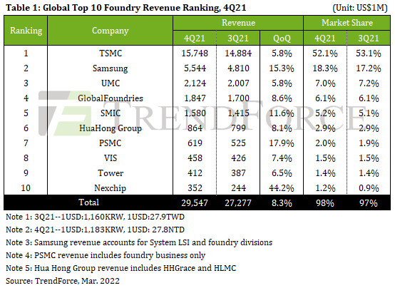
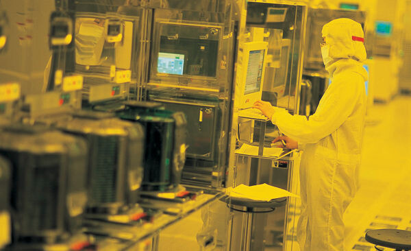
Global Top 10 Foundries Q4 Revenue Up 7.9%, Annual Total Hits US$111.54 Billion in 2023

The latest TrendForce report reveals a notable 7.9% jump in 4Q23 revenue for the world's top ten semiconductor foundries, reaching $30.49 billion. This growth is primarily driven by sustained demand for smartphone components, such as mid and low-end smartphone APs and peripheral PMICs. The launch season for Apple's latest devices also significantly contributed, fueling shipments for the A17 chipset and associated peripheral ICs, including OLED DDIs, CIS, and PMICs. TSMC's premium 3 nm process notably enhanced its revenue contribution, pushing its global market share past the 60% threshold this quarter.

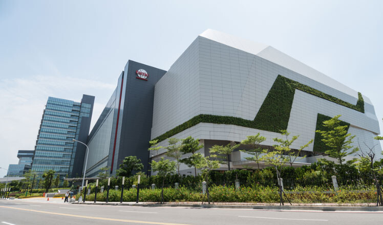
TrendForce remarks that 2023 was a challenging year for foundries, marked by high inventory levels across the supply chain, a weak global economy, and a slow recovery in the Chinese market. These factors led to a downward cycle in the industry, with the top ten foundries experiencing a 13.6% annual drop as revenue reached just $111.54 billion. Nevertheless, 2024 promises a brighter outlook, with AI-driven demand expected to boost annual revenue by 12% to $125.24 billion. TSMC, benefiting from steady advanced process orders, is poised to far exceed the industry average in growth.

Phison Embraces 7 Nanometer: Cooler PCIe Gen 5 SSDs Incoming With New Controller

The current crop of PCIe Gen 5 based M.2 NVMe SSDs run scorching hot to deliver sequential transfer speeds of 10 GB/s, requiring some massive cooling solutions with tiny fans. All this might change, as Phison, a leading SSD controller manufacturer, unveiled three new controllers at the 2024 International CES. One of these that stands out, is the PS5031-E31T, which is built on the 7 nm node, and could power the first Gen 5 SSDs delivering 10 GB/s without elaborate cooling solutions. This is a big upgrade from the 12 nm node used by their first Gen 5 controllers. The PS5031-E31T is a DRAMless controller meant for mainstream Gen 5 SSDs. This controller has a 4-channel flash interface (16 CE), a PCI-Express 5.0 x4 host interface, supports capacities of up to 8 TB, and is claimed by Phison to offer sequential transfer rates of up to 10.8 GB/s, and up to 1500K IOPS random access; exceeding the fastest Gen 4 SSDs.

Phison also updated its high-end controller lineup with the new PS5026-E26 Max14um. This is a variant of the E26 that's designed for the upcoming Micron B58R NAND flash chip that offers 2400 MT/s per channel transfers. Over the 8-channel interface of the E26, this finally unlocks sequential transfer speeds exceeding 14 GB/s reads, and 12.7 GB/s sequential writes. This is merely a revision of the existing E26 with updated power-optimized firmware, the underlying silicon is identical. The E26 Max14um is the first controller to surpass 1000 MB/s in all three PCMark 10 storage tests. We have a sample of an SSD powered by the E26 Max14um in our labs, and will post our review soon.

Top 10 Foundries Post Record 4Q21 Performance for 10th Consecutive Quarter at US$29.55B, Says TrendForce

The output value of the world's top 10 foundries in 4Q21 reached US$29.55 billion, or 8.3% growth QoQ, according to TrendForce's research. This is due to the interaction of two major factors. One is limited growth in overall production capacity. At present, the shortage of certain components for TVs and laptops has eased but there are other peripheral materials derived from mature process such as PMIC, Wi-Fi, and MCU that are still in short supply, precipitating continued fully loaded foundry capacity. Second is rising average selling price (ASP). In the fourth quarter, more expensive wafers were produced in succession led by TSMC and foundries continued to adjust their product mix to increase ASP. In terms of changes in this quarter's top 10 ranking, Nexchip overtook incumbent DB Hitek to clinch 10th place.

TrendForce believes that the output value of the world's top ten foundries will maintain a growth trend in 1Q22 but appreciation in ASP will still be the primary driver of said growth. However, since there are fewer first quarter working days in the Greater China Area due to the Lunar New Year holiday and this is the time when some foundries schedule an annual maintenance period, 1Q22 growth rate will be down slightly compared to 4Q21.

AMD Prepares 7nm "Renoir X" Processors Lacking Integrated Graphics, and "Vermeer S"

AMD apparently finds itself with quite a bit of undigested 7 nm "Renoir" silicon, which it plans to repackage as Socket AM4 processors, reports VideoCardz, citing sources on ChipHell forums. The most interesting aspect of this leak is that the silicon variant, codenamed "Renoir X," comes with a disabled iGPU. This is hence a case of AMD harvesting enough "Renoir" dies with faulty iGPU components, to sell them off as desktop processors. It is also learned that these chips don't feature all of the 8 "Zen 2" CPU cores present on the silicon, but rather AMD is looking to carve out entry-level SKUs, such as the Ryzen 3 or Athlon. The company lacks Athlon desktop SKUs based on "Zen 2" or later, although traditionally the company sought to include some basic iGPU solution with its Athlon SKUs.

In related news, the source reports that AMD will refresh its Ryzen desktop processor family with the new "Vermeer S" Ryzen processors. Built on the existing Socket AM4 package, these use AMD's "Zen 3" CCDs that feature 3D Vertical Cache (3DV Cache), much like the recently announced EPYC "Milan X" server processors. AMD claimed that the 3DV Cache technology has a significant performance uplift on performance akin to a generational update. These could be the company's first response to Intel Core "Alder Lake," although since they're based on the older AM4 platform, could only feature DDR4 and PCIe Gen 4. Much like the Ryzen 3000XT series, these appear to be a stopgap product lineup, with AMD targeting late-Q2/early-Q3 for next-generation "Raphael" Socket AM5 processors based on the "Zen 4" architecture, with DDR5 and PCIe Gen 5.

IBM Unveils New Generation of IBM Power Servers for Frictionless, Scalable Hybrid Cloud

IBM (NYSE: IBM) today announced the new IBM Power E1080 server, the first in a new family of servers based on the new IBM Power10 processor, designed specifically for hybrid cloud environments. The IBM Power10-equipped E1080 server is engineered to be one of the most secured server platforms and is designed to help clients operate a secured, frictionless hybrid cloud experience across their entire IT infrastructure.

The IBM Power E1080 server is launching at a critical time for IT. As organizations around the world continue to adapt to unpredictable changes in consumer behaviors and needs, they need a platform that can deliver their applications and insights securely where and when they need them. The IBM Institute of Business Value's 2021 CEO Study found that, of the 3,000 CEOs surveyed, 56% emphasized the need to enhance operational agility and flexibility when asked what they'll most aggressively pursue over the next two to three years.

IBM Unveils On-Chip Accelerated Artificial Intelligence Processor

At the annual Hot Chips conference, IBM (NYSE: IBM) today unveiled details of the upcoming new IBM Telum Processor, designed to bring deep learning inference to enterprise workloads to help address fraud in real-time. Telum is IBM's first processor that contains on-chip acceleration for AI inferencing while a transaction is taking place. Three years in development, the breakthrough of this new on-chip hardware acceleration is designed to help customers achieve business insights at scale across banking, finance, trading, insurance applications and customer interactions. A Telum-based system is planned for the first half of 2022.

Today, businesses typically apply detection techniques to catch fraud after it occurs, a process that can be time consuming and compute-intensive due to the limitations of today's technology, particularly when fraud analysis and detection is conducted far away from mission critical transactions and data. Due to latency requirements, complex fraud detection often cannot be completed in real-time - meaning a bad actor could have already successfully purchased goods with a stolen credit card before the retailer is aware fraud has taken place.

Penetration Rate of Ice Lake CPUs in Server Market Expected to Surpass 30% by Year's End as x86 Architecture Remains Dominant, Says TrendForce

While the server industry transitions to the latest generation of processors based on the x86 platform, the Intel Ice Lake and AMD Milan CPUs entered mass production earlier this year and were shipped to certain customers, such as North American CSPs and telecommunication companies, at a low volume in 1Q21, according to TrendForce's latest investigations. These processors are expected to begin seeing widespread adoption in the server market in 3Q21. TrendForce believes that Ice Lake represents a step-up in computing performance from the previous generation due to its higher scalability and support for more memory channels. On the other hand, the new normal that emerged in the post-pandemic era is expected to drive clients in the server sector to partially migrate to the Ice Lake platform, whose share in the server market is expected to surpass 30% in 4Q21.

ASRock New BIOS Updates To Support AMD Ryzen 5000 G-Series Desktop Processors with Radeon Graphics

The leading global motherboard, graphics card, and small form factor PC manufacturer, ASRock, has released the latest BIOS that support AMD Ryzen 5000 G-Series Desktop Processors with Radeon Graphics and AMD Ryzen 5000 Series Desktop Processors with PRO Technologies.

AMD Ryzen 5000 G-Series Desktop Processors with Radeon Graphics are the newest generation processors come with industry-leading 7nm technology, elevating processing performance to the next level. And now, ASRock 500-Series, B450 AMD Ryzen motherboards and X300 Mini PC are able to support both of them by updating the latest BIOS.

SiFive Performance P550 Core Sets New Standard as Highest Performance RISC-V Processor IP

SiFive, Inc., the industry leader in RISC-V processors and silicon solutions, today announced launched the new SiFive Performance family of processors. The SiFive Performance family debuts with two new processor cores, the P270, SiFive's first Linux capable processor with full support for the RISC-V vector extension v1.0 rc, and the SiFive Performance P550 core, SiFive's highest performance processor to date. The new SiFive Performance P550 delivers a SPECInt 2006 score of 8.65/GHz, making it the highest performance RISC-V processor available today, and comparable to existing proprietary solutions in the application processor space.

"SiFive Performance is a significant milestone in our commitment to deliver a complete, scalable portfolio of RISC-V cores to customers in all markets who are at the vanguard of SOC design and are dissatisfied with the status quo," said Dr. Yunsup Lee, Co-Founder and CTO of SiFive. "These two new products cover new performance points and a wide range of application areas, from efficient vector processors that easily displace yesterday's SIMD architectures, to the bleeding edge that the P550 represents. SiFive is proud to set the standard for RISC-V processing and is ready to deliver these products to customers today."

Intel Tapes in 7nm Meteor Lake Compute Tile

Intel has today confirmed that they have taped in their upcoming 7 nm Meteor Lake compute tile meaning the design is now ready and Intel can proceed to tape out the whole chip. Intel Meteor Lake is rumored to power the 14th Gen Core series of processors which will launch in 2023 and will feature a 7 nm Enhanced SuperFin node. The Meteor Lake series of processors will be Intel's fourth product series to feature a hybrid core design and will support 600 series chipsets expected to launch later this year for 12th generation Alder Lake processors.
Gregory M. BryantGreat way to start the week! We are taping in our 7 nm Meteor Lake compute tile right now.

A well-deserved celebration by the team on this milestone.

AMD and GlobalFoundries Wafer Supply Agreement Now Non-Exclusive, Paves Way for 7nm sIOD

AMD in a filing with the U.S. Securities and Exchange Commission (SEC), revealed that its wafer supply agreement with GlobalFoundries has been amended. Under the new terms, AMD places orders for wafers from GlobalFoundries up to 2024, with purchase targets set for each year leading up to 2024. Beyond meeting these targets, AMD is free from all other exclusivity commitments. The agreement was previously amended in January 2019, setting annual purchase targets for 2019, 2020, and 2021, while beginning a de-coupling between AMD and GlobalFoundries. This enabled the company to source 7 nm (or smaller) chips, such as CCDs and GPUs, from other foundries, such as TSMC, while keeping GlobalFoundries exclusive for 12 nm (or larger) nodes.

The updated wafer supply agreement unlocks many possibilities for AMD. For starters, it can finally build a next-generation sIOD (server I/O die) on a more efficient node than GlobalFoundries 12LP, such as TSMC 7 nm. This transition to 7 nm will be needed as the next-gen "Genoa" EPYC processor could feature future I/O standards such as DDR5 memory and PCI-Express Gen 5, and the switching fabric for these could be too power-hungry on 12 nm. The "Zen 4" CPU core complex dies (CCDs) of "Genoa" are expected to be built on TSMC 5 nm.

Exxact Launches New Line of Workstations Featuring AMD Ryzen Threadripper PRO Processors

Exxact Corporation, a leading provider of high-performance computing (HPC), artificial intelligence (AI), and data center solutions, announced their new line of Valence and TENSOREX Workstations featuring the new AMD Ryzen Threadripper PRO Processors. These professional grade workstations geared towards engineers, visual graphic artists, and scientists provide game changing single and multithreaded performance and provide unrivaled memory bandwidth1. Exxact has positioned itself to be one of the first system integrators to provide workstations equipped with these powerful new processors.

"The new AMD Ryzen Threadripper PRO Processors are a massive leap forward for engineers, designers, architects, any professional who demands ultimate performance and security from their workstation," said Jason Chen, Vice President at Exxact Corporation. "By being one of the first companies to offer these workstations, our customers can gain the competitive edge in their industry," added Jason.

Intel's Manufacturing Outlook for the Future Doesn't Inspire Confidence in Successful Competition, According to Susquehanna Call

Susquehanna is a global trading firm which has various interests in silicon manufacturing - and part of that interest is naturally materialized in Intel. In a recent group call from the firm, some details on Intel's manufacturing and product design woes came to light, which point towards even more execution slips than we've already seen. During the call, a number of points were broached, including dismal yields for Intel's 10 nm manufacturing process as of its introduction in late 2018 (which is why it never saw mainstream adoption from the company). News that Intel is looking for a new CEO also don't instill confidence on current CEO Bob Swan's capacity to steer the Intel behemoth.

Improved yields on 10 nm are being reported due to deployment of Intel's SuperFin technology, which improved yields to upwards of 50%, but still keeps them under the ones achieved in Intel's 14 nm process; an eye-opening tidbit in that Cannon Lake on 10 nm originally saw yields of only 25% usable chips per wafer; and that backporting Rocket Lake meant Intel had to deal with unfathomably large chips and high power consumption characteristics. And to add insult to injury, there is still not a definite timetable for 7 nm deployment, with delays being expected to be worse than the previously reported 6-12 months. This all paints a somewhat grim picture for Intel's capacity to compete with TSMC-powered AMD in many of its most important markets; the blue giant won't topple, of course, but it's expected that five years from now, we'll be looking at a very different outlook in the market between AMD and Intel. You can check the talked-about points in the call via the transcript after the break. You should still take the transcript with a grain of salt.

China Forecast to Represent 22% of the Foundry Market in 2020, says IC Insights

IC Insights recently released its September Update to the 2020 McClean Report that presented the second of a two-part analysis on the global IC foundry industry and included a look at the pure-play foundry market by region.

China was responsible for essentially all of the total pure-play foundry market increase in 2018. In 2019, the U.S./China trade war slowed China's economic growth but its foundry marketshare still increased by two percentage points to 21%. Moreover, despite the Covid-19 shutdown of China's economy earlier this year, China's share of the pure-play foundry market is forecast to be 22% in 2020, 17 percentage points greater than it registered in 2010 (Figure 1).

Rambus Advances HBM2E Performance to 4.0 Gbps for AI/ML Training Applications

Rambus Inc. (NASDAQ: RMBS), a premier silicon IP and chip provider making data faster and safer, today announced it has achieved a record 4 Gbps performance with the Rambus HBM2E memory interface solution consisting of a fully-integrated PHY and controller. Paired with the industry's fastest HBM2E DRAM from SK hynix operating at 3.6 Gbps, the solution can deliver 460 GB/s of bandwidth from a single HBM2E device. This performance meets the terabyte-scale bandwidth needs of accelerators targeting the most demanding AI/ML training and high-performance computing (HPC) applications.

"With this achievement by Rambus, designers of AI and HPC systems can now implement systems using the world's fastest HBM2E DRAM running at 3.6 Gbps from SK hynix," said Uksong Kang, vice president of product planning at SK hynix. "In July, we announced full-scale mass-production of HBM2E for state-of-the-art computing applications demanding the highest bandwidth available."

TSMC Details 3nm N3, 5nm N5, and 3DFabric Technology

TSMC on Monday kicked off a virtual tech symposium, where it announced its new 12 nm N12e node for IoT edge devices, announced the new 3DFabric Technology, and detailed progress on its upcoming 5 nm N5 and 3 nm N3 silicon fabrication nodes. The company maintains that the N5 (5 nm) node offers the benefits of a full node uplift over its current-gen N7 (7 nm), which recently clocked over 1 billion chips shipped. The N5 node incorporates EUV lithography more extensively than N6/N7+, and in comparison to N7 offers 30% better power at the same performance, 15% more performance at the same power, and an 80% increase in logic density. The company has commenced high-volume manufacturing on this node.

2021 will see the introduction and ramp-up of the N5P node, an enhancement of the 5 nm N5 node, offering a 10% improvement in power at the same performance, or 5% increase in performance at the same power. A nodelet of the N5 family of nodes, called N4, could see risk production in Q4 2021. The N4 node is advertised as "4 nm," although the company didn't get into its iso-power/iso-performance specifics over the N5 node. The next major node for TSMC will be the 3 nm N3 node, with massive 25%-30% improvement in power at the same performance, or 10%-15% improvement in performance at same power, compared to N5. It also offers a 70% logic density gain over N5. 3DFabric technology is a new umbrella term for TSMC's CoWoS (chip on wafer on substrate), CoW (chip on wafer), and WoW (wafer on wafer) 3-D packaging innovations, with which it plans to offer packaging innovations that compete with Intel's various new 3D chip packaging technologies on the anvil.

TSMC Ships its 1 Billionth 7nm Chip

In a bid to show off its volume production prowess and technological edge (but mostly to rub it in to rival fabs), TSMC on Thursday announced that it shipped its 1 billionth chip fabricated on its 7 nm process. If these dies were combined into one big rectangular wafer, they would cover 13 New York City blocks. TSMC's 7 nm process debuted with its N7 node, which went into volume production in April 2018, over two years ago. The fab has since mass-produced 7 nm chips for the likes of Qualcomm, Apple, and AMD, among dozens of other clients. The company now looks to monetize refinements of N7, namely the N7e and N7P (DUV refinements), while executing its crucial EUV-based N7+ node, leading up to future nodelets such as N6. Much of TSMC's growth will be propelled by 5G modems, application processors, and its pivotal role in the growth of companies such as AMD.

MediaTek Introduces Dimensity 800U 5G SoC

MediaTek today announced its newest 5G SoC, the Dimensity 800U, as the latest addition in MediaTek's Dimensity series family. The 7 nm Dimensity 800U chipset is designed for multi-core high performance and leading 5G+5G Dual Sim Dual Standby (DSDS) technology. With Dimensity 800U MediaTek continues to accelerate the rollout of 5G technology and deliver premium experiences on mid-tier 5G smartphones.

"MediaTek has always focused on enhancing the user experience with our leading semiconductor technology, whether consumers are streaming, gaming or taking photos," said Dr. Yenchi Lee, Deputy General Manager of MediaTek's Wireless Communications Business Unit. "MediaTek's Dimensity 800U brings cutting-edge, next-gen technology to the Dimensity SoC series, bringing MediaTek's advanced 5G, imaging and multimedia technologies to high-performance 5G smartphones that deliver incredible 5G experiences."

Intel to Detail Xe Graphics on August 13

Intel is expected to reveal technical details of its upcoming Xe graphics architecture on August 13, according to a tweet by Intel Graphics that has since been deleted. Tom's Hardware believes the reveal is still on the cards. "You've waited. You've wondered. We'll deliver. In 20 days, expect more details on Xe graphics," the tweet read. Senior Fellow and Director of Graphics Architecture at Intel, David Blythe is expected to present a technical brief on the Xe graphics architecture at a Hot Chips 2020 virtual event on August 17.

These technical reveals are closely timed with the launch of "Tiger Lake," Intel's first commercial debut of Xe as an iGPU solution the chipmaker refers to as "Gen12" for consistency with older generations of integrated graphics. Xe is far from designed for just iGPU or small dGPUs, with the architecture being scalable all the way up to large scalar compute processors the size of beer mug coasters. Even as an iGPU, Xe is formidable, as it was recently shown playing AAA games by itself. Recent commentary from Intel at its Q2 2020 financial results provided strong hints of Xe dGPUs being de-coupled from Intel's foundry woes, and possibly headed for third-party foundries such as Samsung or TSMC.

Intel 7nm CPUs Delayed by a Year, Alder Lake in 2H-2021, Other Commentary from Intel Management

Intel's silicon fabrication woes refuse to torment the company's product roadmaps, with the company disclosing in its Q2-2020 financial results release that the company's first CPUs built on the 7 nanometer silicon fabrication node are delayed by a year due to a further 6-month delay from prior expectations. The company will focus on getting its 10 nm node up to scale in the meantime.

The company mentioned that the 10 nm "Tiger Lake" mobile processor and "Ice Lake-SP" enterprise processor remains on-track for 2020. The company's 12th Generation Core "Alder Lake-S" desktop processors won't arrive before the second half of 2021. In the meantime, Intel will launch its 11th Gen Core "Rocket Lake" processor on the 14 nm node, but with increased IPC from the new "Cypress Cove" CPU cores. Also in 2H-2021, the company will launch its "Sapphire Rapids" enterprise processors that come with next-gen connectivity and updated CPU cores.
Intel 7 nanometer delay

New AMD Radeon Pro 5600M Mobile GPU Brings Desktop-Class Graphics Performance and Enhanced Power Efficiency to 16-inch MacBook Pro

AMD today announced availability of the new AMD Radeon Pro 5600M mobile GPU for the 16-inch MacBook Pro. Designed to deliver desktop-class graphics performance in an efficient mobile form factor, this new GPU powers computationally heavy workloads, enabling pro users to maximize productivity while on-the-go.

The AMD Radeon Pro 5600M GPU is built upon industry-leading 7 nm process technology and advanced AMD RDNA architecture to power a diverse range of pro applications, including video editing, color grading, application development, game creation and more. With 40 compute units and 8 GB of ultra-fast, low-power High Bandwidth Memory (HBM2), the AMD Radeon Pro 5600M GPU delivers superfast performance and excellent power efficiency in a single GPU package.

Samsung Expands its Foundry Capacity with A New Production Line in Pyeongtaek

Samsung Electronics Co., Ltd., a world leader in advanced semiconductor technology, today announced plans to boost its foundry capacity at the company's new production line in Pyeongtaek, Korea, to meet growing global demand for cutting-edge extreme ultraviolet (EUV) solutions.

The new foundry line, which will focus on EUV-based 5 nanometer (nm) and below process technology, has just commenced construction this month and is expected to be in full operation in the second half of 2021. It will play a pivotal role as Samsung aims to expand the use of state-of-the-art process technologies across a myriad of current and next generation applications, including 5G, high-performance computing (HPC) and artificial intelligence (AI).

Lenovo Announces ThinkPad Laptops Powered by AMD Ryzen PRO 4000

Today, Lenovo announced the new ThinkPad E14 and E15 with up to AMD Ryzen 7 4700U processors with Radeon Graphics bringing an improved design, higher performance and enhanced productivity features for SMB customers. Also, selected ThinkPad T, X and L series powered by AMD Ryzen PRO 4000 Series Mobile Processors announced in February are coming very soon. Delivering smarter IT innovations for better user experiences, the latest ThinkPad models meet today's increasing remote working needs.

Engineered for effortless productivity virtually anywhere, the new ThinkPad E14 and E15 offers a smart choice for SMB decision makers. An updated design with an improved screen to body ratio of 85%, the E series also offers the security and durability needed in a changing world. Innovative security features are provided on ThinkPad E series for the first time, including a touch fingerprint reader and an optional IR camera with Glance by Mirametrix technology. The touch fingerprint reader integrated into the power button offers one touch power and logon. The software-enabled Glance feature responds to users' presence, automatically locking the laptop when the user steps away, and also offers a Snap Window and Smart Pointer function for multi display setups.

TSMC Secures Orders from NVIDIA for 7nm and 5nm Chips

TSMC has reportedly secured orders from NVIDIA for chips based on its 7 nm and 5 nm silicon fabrication nodes, sources tell DigiTimes. If true, it could confirm rumors of NVIDIA splitting its next-generation GPU manufacturing between TSMC and Samsung. The Korean semiconductor giant is commencing 5 nm EUV mass production within Q2-2020, and NVIDIA is expected to be one of its customers. NVIDIA is expected to shed light on its next-gen graphics architecture at the GTC 2020 online event held later this month. With its "Turing" architecture approaching six quarters of market presence, it's likely that the decks are being cleared for a new architecture not just in HPC/AI compute product segment, but also GeForce and Quadro consumer graphics cards. Splitting manufacturing between TSMC and Samsung would help NVIDIA disperse any yield issue arriving from either foundry's EUV node, and give it greater bargaining power with both.

SMIC 7nm-class N+1 Foundry Node Going Live by Q4-2020

China's state-backed SMIC (Semiconductor Manufacturing International Corporation) has set an ambitious target of Q4-2020 for its 7 nanometer-class N+1 foundry node to go live, achieving "small scale production," according to a cnTechPost report. The company has a lot of weight on its shoulders as geopolitical hostility between the U.S. and China threatens to derail the country's plans to dominate 5G technology markets around the world. The SMIC N+1 node is designed to improve performance by 20%, reduce chip power consumption by 57%, reduce logic area by 63%, and reduce SoC area by 55%, in comparison to the SMIC's 14 nm FinFET node, Chinese press reports citing a statement from SMIC's co-CEO Dr. Liang Mengsong.

Dr. Liang confirmed that the N+1 7 nm node and its immediate successor will not use EUV lithography. N+1 will receive a refinement in the form of N+2, with modest chip power consumption improvement goals compared to N+1. This is similar to SMIC's 12 nm FinFET node being a refinement of its 14 nm FinFET node. Later down its lifecycle, once the company has got a handle of its EUV lithography equipment, N+2 could receive various photomasks, including a switch to EUV at scale.
Return to Keyword Browsing
Apr 19th, 2024 14:39 EDT change timezone

New Forum Posts

Popular Reviews

Controversial News Posts