News Posts matching #96-layer

Return to Keyword Browsing

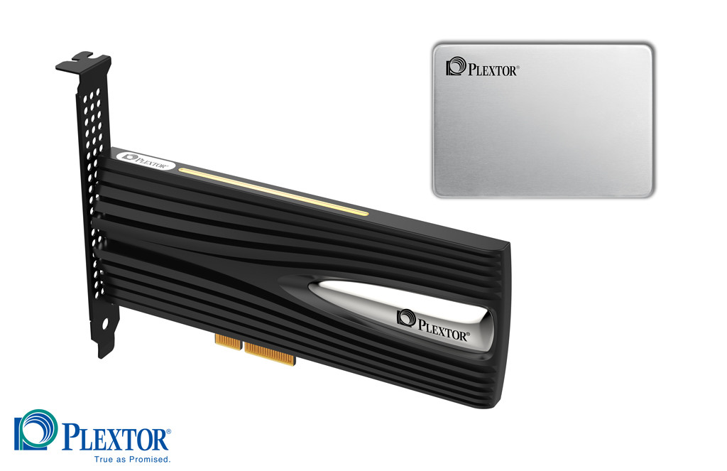
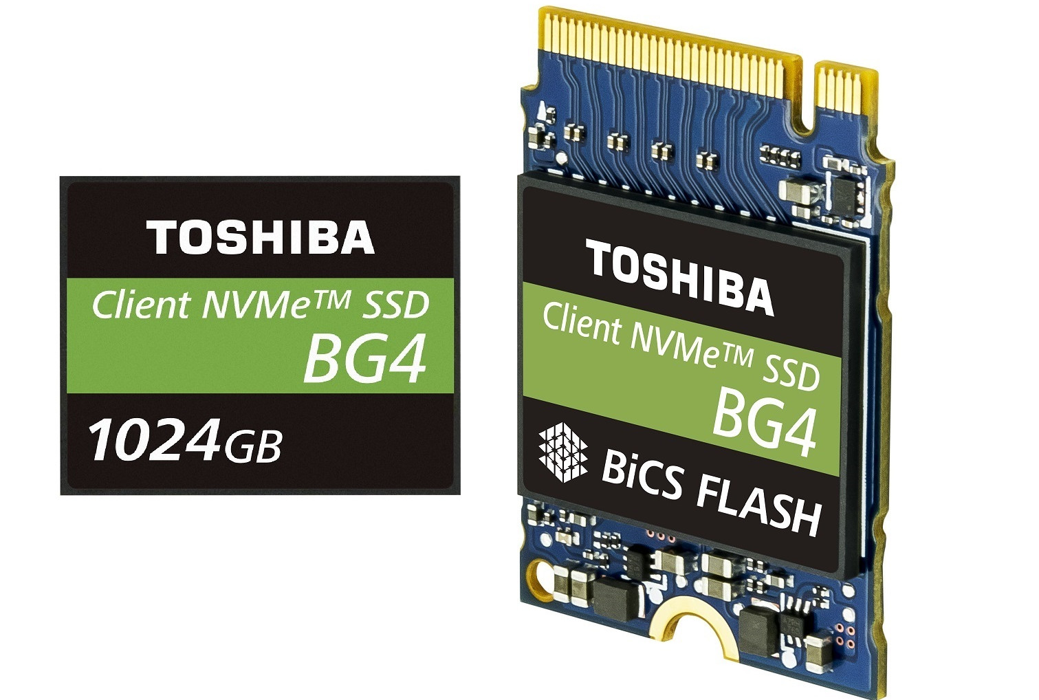
2019 the Year of 1TB SSDs: Prices Fall by 50%

1-Terabyte SSDs could become a new mainstream-desktop must-have in 2019, as prices of the drives have fallen by 50 percent year-over-year, according to DigiTimes. A 1 TB SATA SSD in the 2.5-inch form-factor can now be had for as little as $99, while faster NVMe drives in the M.2 form-factor start around $130. At the beginning of 2018, 1 TB SATA SSDs used to start around the $160-mark, and NVMe drives north of $200. The 1 TB category includes 960 GB, 1000 GB, and 1024 GB marketed capacities with varying amounts of overprovisioning set by manufacturers.

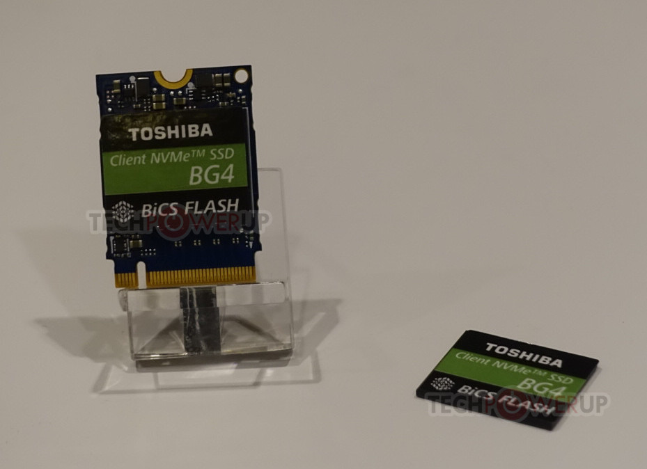
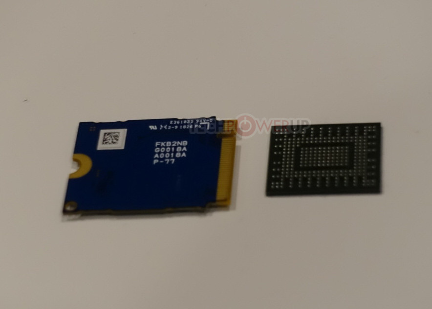
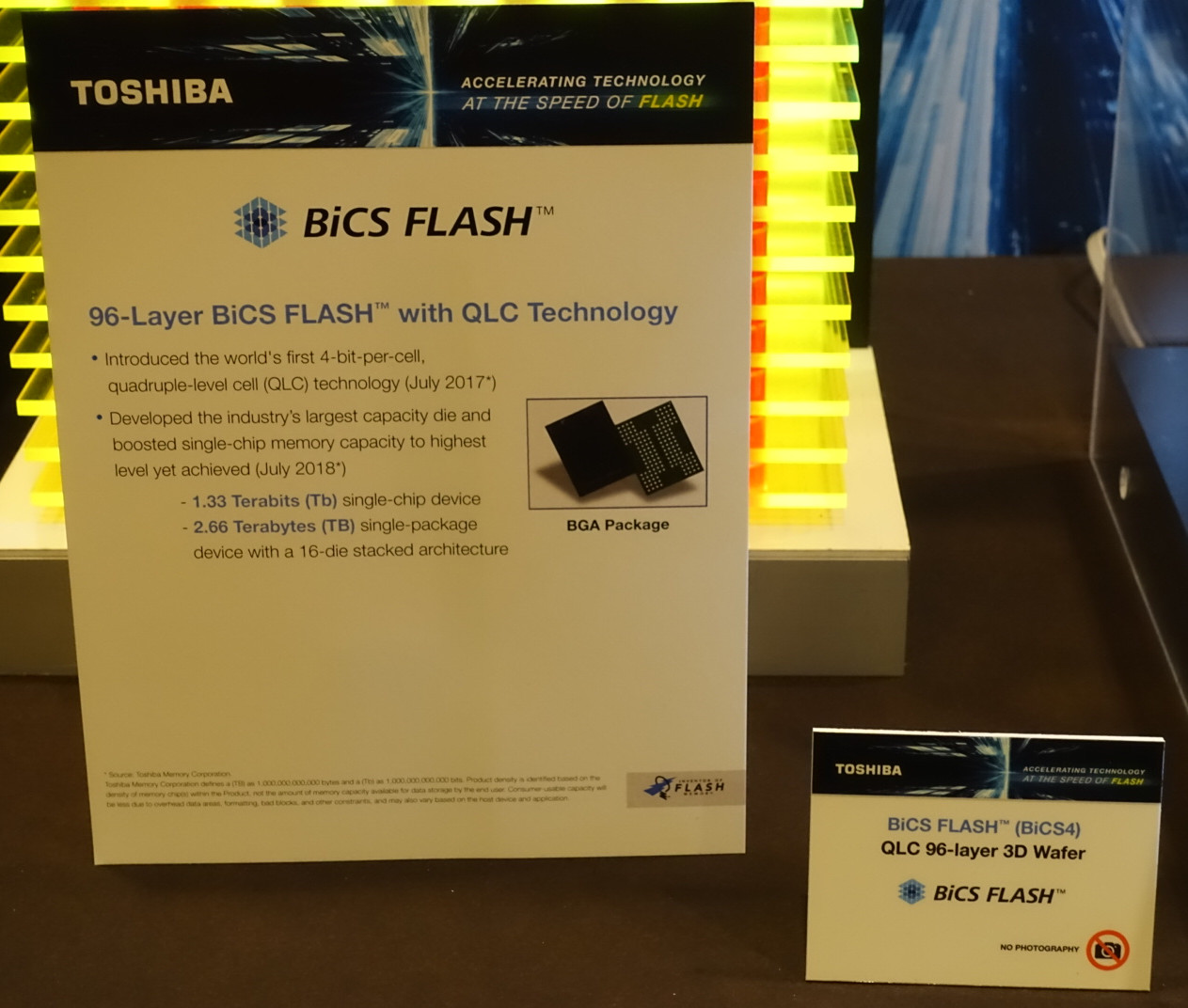
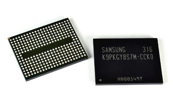
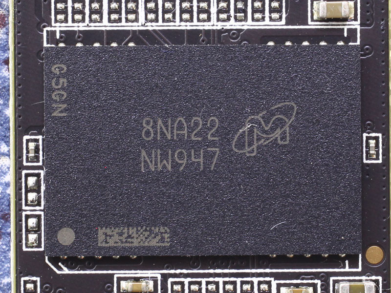
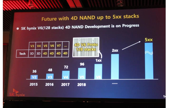
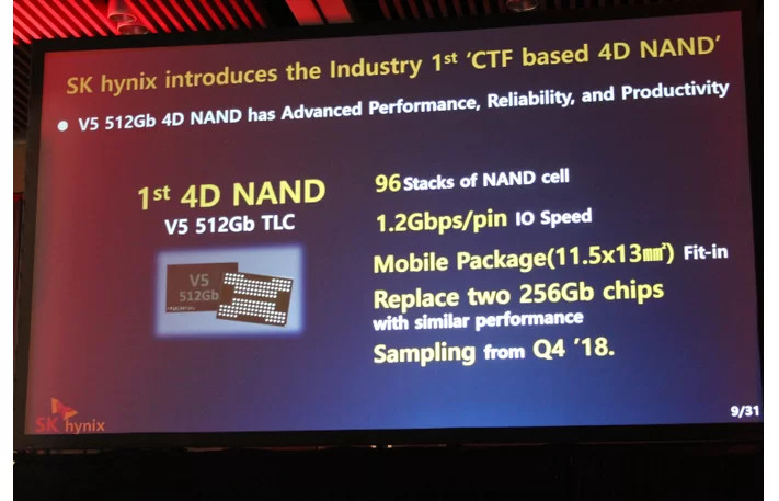
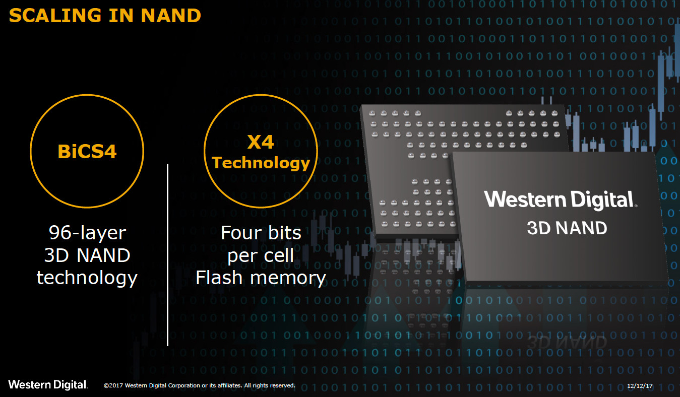
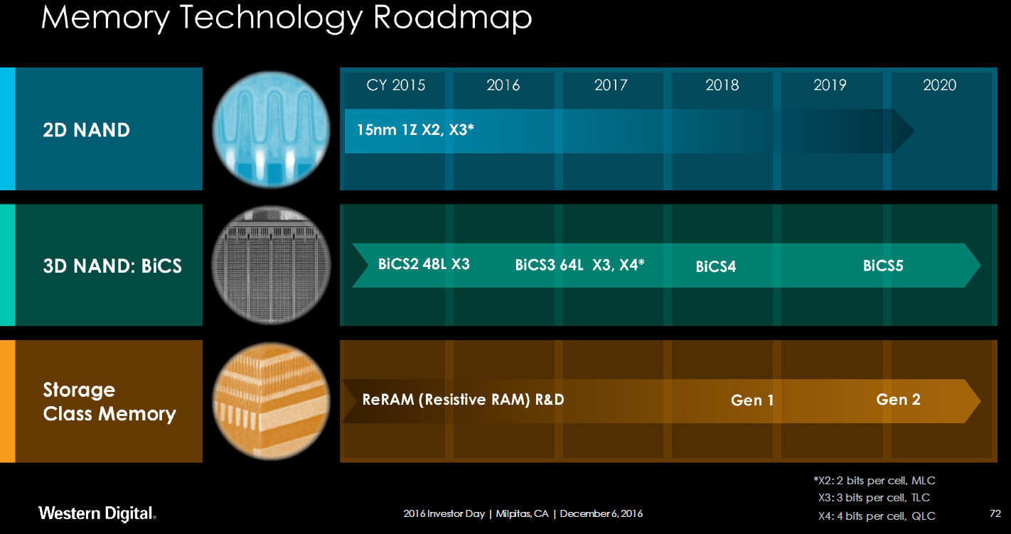
Falling SSD prices are accelerated by the entry of cost-effective 96-layer 3D NAND flash, higher-density QLC NAND flash, undigested inventories of drives based on older technologies such as 64-layer or TLC NAND flash; and a 15 percent sequential quarterly drop in NAND flash prices in the industry. Growth in speeds of client-segment SSDs have remained largely flat over the year, and not much is to be expected in performance growth other than perhaps the advent of PCIe gen 4.0 based enterprise SSDs towards the end of the year.

Toshiba Unveils Industry's First UFS Ver. 3.0 Embedded Flash Memory Devices

Toshiba Memory Corporation, the world leader in memory solutions, has started sampling[1] the industry's first Universal Flash Storage (UFS) Ver. 3.0 embedded flash memory devices. The new line-up utilizes the company's cutting-edge, 96-layer BiCS FLASH 3D flash memory and is available in three capacities: 128GB, 256GB and 512GB. With high-speed read/write performance and low power consumption, the new devices are suitable for applications such as mobile devices, smartphones, tablets, and augmented/virtual reality systems.

The new devices integrate 96-layer BiCS FLASH 3D flash memory and a controller in a JEDEC-standard 11.5 x 13.0 mm package. The controller performs error correction, wear leveling, logical-to-physical address translation and bad-block management for simplified system development.

PLEXTOR Debuts Next-Gen Consumer SSDs at CES 2019

PLEXTOR, a leading developer of award-winning solid-state drives (SSDs) and other high-performance digital storage devices, today announced the introduction of its latest line of PCIe and SATA SSDs at this year's CES.

The new M10Pe PCIe SSD Series offers a new level of speed and performance targeted for all PC gamers and applications intensive users. The new series combines advanced 96-layer 3D NAND flash and industry leading controller to deliver awesome sequential read/write speeds up to 3,200/2,500 MB/s and random read/write speeds up to 410,000/320,000 IOPS.

Toshiba Shows Off 96-Layer BiCS FLASH Alongside Plethora of Enterprise SSDs at CES 2019

During our visit with Toshiba at CES 2019, we were shown not only new technologies that they will be rapidly deploying but a large number of SSDs for various market segments. The biggest draw was their 96-layer BiCS Flash with 4-bit-per-cell quadruple-level cell (QLC) technology. Toshiba is now pushing the boundary for capacity as a single chip device can reach 1.33 Tb (Terabits) while a single package device with 16-dies stacked architecture can reach 2.66 TB. That said, they are already sampling their 1 TB NVMe single package BG4 series SSDs to PC OEM customers in limited quantities.

These latest drives with their new BiCS FLASH technology incorporate everything into a tiny SSD that offers class-leading storage with sequential read performance reaching up to 2250 MB/s. Random read performance can also hit exceptional levels reaching up to 380,000 IOPS. For now, these BG4 based drives are targeted at ultra-thin PC notebooks, IoT embedded systems and will be made available in four capacities including; 128 GB, 256 GB, 512 GB and finally 1 TB. To meet expected demand, Toshiba will also be opening a facility in Japan dedicated to this latest technology in order to bring even higher capacities per NAND module.

Toshiba Memory Unveils 1TB Single Package PCIe Gen3 x4 SSD with 96-Layer 3D Flash

Toshiba Memory Corporation, the world leader in memory solutions, today announced the BG4 series, a new line-up of single package NVMe SSDs with capacities up to 1,024 GB, which places both innovative 96-layer 3D flash memory and an all-new controller into one package to deliver best-in-class read performance. The BG4 series is currently sampling to PC OEM customers in limited quantities, with general sample availability expected later in the second calendar quarter of 2019.

This new series of single package SSDs, featuring PCIe Gen 3.0 x4 lanes, offers sequential read performance up to 2,250 MB/s, and with improved flash management delivers industry-leading random read performance up to 380,000 IOPS. The BG4 single package SSDs are suitable for compact and performance-oriented systems, such as ultra-thin PC notebooks, IoT embedded systems and server boot in data centers.

SK Hynix Launches World's First 'CTF-based 4D NAND Flash' (96-Layer 512Gb TLC)

SK Hynix today launched the world's first 96-Layer 512Gb CTF (Charge Trap Flash) based 4D NAND flash. Don't let the name trick you - it's still based on 3D TLC technology, but SK Hynix has gone and added a 4th dimension due to its pairing of charge trap flash technology in conjunction with PUC (Peri. Under Cell technology.

SK Hynix says that their approach is (obviously) better than the industry-wide 3D Floating Gate approach. The 4D NAND chip design results in a reduction of more than 30% in chip size, and increases bit productivity per wafer by 49% compared to the Company's 72-Layer 512Gb 3D NAND. Moreover, the product has 30% higher write and 25% higher read performance. Also, its data bandwidth is doubled to an industry-leading (in size) 64KB. Data I/O (Input Output) speed reaches 1,200Mbps (Megabits/sec) at 1.2 V.

Samsung Cuts CAPEX by a Quarter, Calls it an "End of the Chip Boom"

Samsung Electronics Wednesday slashed its capital expenditure (capex) by a quarter, which could significantly reduce its NAND flash chip output, and raise NAND flash prices back to profitability for the company, although not anytime soon. This could herald a rise in SSD prices around this time next year, although they partly contradict analyses that predict further slides in NAND flash prices through 2019, as the advent of 96-layer 3D QLC NAND flash by every major player would add to swelling inventories in the market. If you'll recall, Samsung reportedly desires DRAM prices to remain high and establish current high DRAM prices as a new normal. The company went as far as to further reduce its DRAM output, just so supplies of DRAM in the market remain low. The company remarked that acceleration in NAND flash price-drops signifies an end of the "boom" in NAND flash chip demand that fueled growth over the past two years, as justification to its capex cuts.

NAND Flash Prices May See Further Drops in 2019, DRAM to Remain Flat

Solid-state drives are cheaper than ever, thanks to systematic decline in NAND flash prices owing both to oversupply and increases in densities. NAND flash prices have already declined by 50 percent over 2018, according to a DigiTimes report, and will continue to slide through 2019. ADATA chairman Simon Chen commented that NAND flash makers haven't slowed down capacity expansions, and 2019 could witness an even bigger drop in prices than 2018.

Major NAND flash makers such as IMFlash Technology, SK Hynix, Samsung, Western Digital, Toshiba, have already taped out their 96-layer 3D NAND flash products, which could enter volume production in the first half of 2019. This could impact prices of existing swelling inventories of products based on 64-layer NAND flash. In theory, the 96-layer chips introduce 50 percent increases in densities. Adoption of newer technologies such as QLC (4 bits per cell) will expand densities even further. The same report also projects that DRAM prices could largely remain flat throughout 2019. Most NAND flash makers also happen to make DRAM, and could balance their NAND flash losses with DRAM profits.

Toshiba Memory and Western Digital Celebrate the Opening of Fab 6

Toshiba Memory Corporation and Western Digital Corporation today celebrated the opening of a new state-of-the-art semiconductor fabrication facility, Fab 6, and the Memory R&D Center, at Yokkaichi operations in Mie Prefecture, Japan. Toshiba Memory started construction of Fab 6, a dedicated 3D flash memory fabrication facility, in February 2017. Toshiba Memory and Western Digital have installed cutting-edge manufacturing equipment for key production processes including deposition and etching. Mass production of 96-layer 3D flash memory utilizing the new fab began earlier this month.

Demand for 3D flash memory is growing for enterprise servers, data centers and smartphones, and is expected to continue to expand in the years ahead. Further investments to expand its production will be made in line with market trends. The Memory R&D Center, located adjacent to Fab 6, began operations in March of this year, and will explore and promote advances in the development of 3D flash memory. Toshiba Memory and Western Digital will continue to cultivate and extend their leadership in the memory business by actively developing initiatives aimed at strengthening competitiveness, advancing joint development of 3D flash memory, and making capital investments according to market trends.

SK Hynix Unveils 4D NAND Flash Memory Concept

3D NAND flash revolutionized flash storage as it used the third dimension (height) to stack multiple NAND flash layers, resulting in infinitesimally smaller footprint and reduced costs. SK Hynix believes that a "4-dimensional" NAND flash package is possible. Don't worry, such a stack doesn't look like a tesseract. Conventional 3D NAND flash relies on stacks of charge-trap flash (CTF) cells spatially located alongside its periphery block (which is responsible for wiring out each of the layers of the CTF stack). On a 2-D plane you'd be spending substrate real-estate on both the CTF and periphery block.

SK Hynix believes that the periphery block can be stacked along with the CTF stack, with microscopic vias wiring up the stack along the periphery, reducing the footprint of each cell stack. 4D stacking will also allow for greater number of CTF stacks per cell. Just to be clear, we're talking about stacks of cell and not stacks of NAND flash dies. The V5 cell-stack in SK Hynix's design entails 4 cells and periphery blocks sandwiched. The first implementation of this technology is a 96-layer 4D NAND flash chip with 512 Gb of capacity and TLC (3 bits per cell) density, although the technology is ready for QLC cells. This 512 Gb chip will begin sampling by the end of 2018, and the company is already working on a 1 Tb chip for 2019.

Western Digital Releases 96-layer 3D QLC NAND with 1.33 Tb Capacity

Western Digital Corp. today announced successful development of its second-generation, four-bits-per-cell architecture for 3D NAND. Implemented for the company's 96-layer BiCS4 device, the QLC technology delivers the industry's highest 3D NAND storage capacity of 1.33 terabits (Tb) in a single chip. BiCS4 was developed at the joint venture flash manufacturing facility in Yokkaichi, Japan with our partner Toshiba Memory Corporation. It is sampling now and volume shipments are expected to commence this calendar year beginning with consumer products marketed under the SanDisk brand. The company expects to deploy BiCS4 in a wide variety of applications from retail to enterprise SSDs.

Toshiba Develops 96-layer BiCS FLASH with QLC Technology

Toshiba Memory Corporation, the world leader in memory solutions, today announced that it has developed a prototype sample of 96-layer BiCS FLASH, its proprietary 3D flash memory, with 4-bit-per-cell (quad level cell, QLC) technology that boosts single-chip memory capacity to the highest level yet achieved.Toshiba Memory will start to deliver samples to SSD and SSD controller manufacturers for evaluation from the beginning of September, and expects to start mass production in 2019.

The advantage of QLC technology is pushing the bit count for data per memory cell from three to four and significantly expanding capacity. The new product achieves the industry's maximum capacity of 1.33 terabits for a single chip which was jointly developed with Western Digital Corporation. This also realizes an unparalleled capacity of 2.66 terabytes with a 16-chip stacked architecture in one package. The huge volumes of data generated by mobile terminals and the like continue to increase with the spread of SNS and progress in IoT, and the need to analyze and utilize that data in real time is expected to increase dramatically. That will require even faster than HDD, larger capacity storage and QLC products using the 96-layer process will contribute a solution.

Micron Ready With 96-Layer Flash & 1Y nm DRAM in 2H 2018

In their recent earnings call, Micron commented that they have 96-layer 3D NAND technology on track for volume shipments in the second half of 2018. Most of today's SSDs typically use 32-layer technology, with 64-layer flash chips used in some recent releases like the Crucial MX500. 96-layer is the third generation of 3D NAND and increases storage capacity per chip even further which allows smaller and more energy efficient mobile devices to be built. Of course it will be cheaper too, compared to current-generation 64 layer NAND, which should bring SSD pricing down even more, and of course generally help pricing of consumer products which use flash memory.

The second important note from the presentation is that Micron expects 1X nm (18 nm) DRAM production to exceed that of previous generations before the end of this year. Their next-generation 1Y nm (15/16 nm) DRAM is on track to begin production shipments in the second half of 2018, too. As they noted in a previous event, their product and process roadmap for DRAM 1z looks solid and 1-alpha development programs already under way.

Marvell Launches New 88SS1084 and 88SS1100 NVMe SSD Controllers

Marvell, a leader in storage, networking and connectivity semiconductor solutions, today announced its latest NVM Express (NVMe ) solid-state drive (SSD) controller family for mainstream and high-performance PC client and edge computing SSDs. The Gen 3x4 PCIe SSD controllers, the 4-channel 88SS1084 and 8-channel 88SS1100, bring leading performance, endurance and reliability to the industry and will help broaden the adoption of NVMe SSDs across emerging client and edge computing applications. The controllers integrate Marvell's fourth generation of NANDEdge technology, offering the advanced error correction capabilities to address the increasing demands required to enable future SSD solutions with emerging 96-layer triple level-cell (TLC) and quad level-cell(QLC) NAND architectures.

As gaming, video-on-demand, CAD, imaging, photography and video surveillance proliferate and scale, NVMe SSDs can meet the increasing storage performance and capacity requirements that these end use applications seek. The new Marvell client NVMe SSD controller family can provide up to 3.6GB/s of bandwidth and up to 700,000 input output per second (IOPS). The 88SS1084 and 88SS1100 devices can save system power consumption by supporting lower voltage NAND devices and LPDDR4 DRAM components. These features enable PCs and edge computing devices to process and store increasingly data-intensive workloads more quickly and reliably.

Western Digital Reinforces Commitment to 96-layer, BiCS4 3D NAND

Even as researchers expect 3D NAND flash to achieve the 140-layer level by 2021, technology and manufacturers still have to take all the intermediate steps before we're actually there. In that sense, Western Digital has just announced that they're well on their way in producing 96-layer 3D NAND and distributing it to customers. For now, the memory will be used for inexpensive storage solutions, but the idea is to eventually ramp um production for other, higher-performance products.

Western Digital CEO Steve Milligan kept the production ramp-up (and the expectation of BiCS4 production eventually surpassing BiCS3) under wraps, but it seems all is going well with the production. He added that "(...) if you look to where we at from a yield curve perspective, because [BICS4] is not too mature, we are very pleased with where we are. Because once you get to a certain point, you can project where you are going to end at (based on cycles of learning, etc)." As announced by Western Digital before, it's likely this initial production run is delivering 256 Gb capacity chips, with improvements in yields to allow for increased capacity down the road, eventually, up to 1 Tb capacity per chip.
Return to Keyword Browsing
Apr 23rd, 2024 12:56 EDT change timezone

New Forum Posts

Popular Reviews

Controversial News Posts