News Posts matching #ASIC

Return to Keyword Browsing

TSMC to Execute Bitmain's Orders for 5nm Crypto-Mining ASICs from Q3-2021

TSMC will be manufacturing next-generation 5 nm ASICs for Bitmain. The company designs purpose-built machines for mining crypto-currency, using ASICs. DigiTimes reports that the 5 nm volume production could kick off form Q3-2021. Bitmain's latest Antminer ASIC-based mining machines announced last month were purported to be up to 32 times faster than a GeForce RTX 3080 at mining Ethereum. Recent history has shown that whenever ASICs catch up or beat GPUs at mining, prices of GPUs tend to drop. With no 5 nm GPUs on the horizon for Q3-2021, one really can expect market pressure from crypto-miners to drop off when Antminers gain traction.

Xilinx Reports Fiscal Fourth Quarter and Fiscal Year 2021 Results

Xilinx, Inc. (Nasdaq: XLNX), the leader in adaptive computing, today announced record revenues of $851 million for the fiscal fourth quarter, up 6% over the previous quarter and an increase of 13% year over year. Fiscal 2021 revenues were $3.15 billion, largely flat from the prior fiscal year. GAAP net income for the fiscal fourth quarter was $188 million, or $0.75 per diluted share. Non-GAAP net income for the quarter was $204 million, or $0.82 per diluted share. GAAP net income for fiscal year 2021 was $647 million, or $2.62 per diluted share. Non-GAAP net income for fiscal year 2021 was $762 million, or $3.08 per diluted share.

Additional fourth quarter of fiscal year 2021 comparisons are provided in the charts below. "We are pleased with our fourth quarter results as we delivered record revenues and double-digit year-over-year growth in the midst of a challenging supply chain environment," said Victor Peng, Xilinx president and CEO. "Xilinx saw further improvement in demand across a majority of our diversified end markets with key strength in our Wireless, Data Center and Automotive markets, the pillars of our growth strategy. Our teams have executed well and we remain focused on continuing to meet customers' critical needs.

Team Group Announces T-CREATE EXPERT NVMe SSD with Extreme 12,000 TBW Endurance

In recent years, the cryptocurrency market has been gaining a great deal of attention, leading to a continuous surge in global mining. Chia, started trading in May, is one of the new types of cryptocurrencies. Its mining method is different from previous cryptocurrencies that use GPUs and ASICs to complete calculations and earn profits. The everlastingly durability EXPERT PCIe SSD, developed by TEAMGROUP's creator sub-brand T-CREATE, is the best choice for the environmentally-friendly "storage capacity mining" that Chia promotes.

The Chia Network utilizes a consensus algorithm called "Proof of Space and Time." A Chia farmer's possible yield is directly proportional to their amount of storage space. If you want to earn higher profits today, you need to have more hard drive space. This approach ensures that no one will design special-purpose hardware (ASIC) for mining it. Storage capacity and power consumption are also relatively unrelated. Therefore, Chia Network is a new "green" currency system. If you want to join the mining community utilizing this environmentally-friendly model, T-CREATE EXPERT PCIe SSD can help you get the greatest results. It features spectacular TBW values of up 12,000 TB, making it the perfect tool for supporting the intense write-cycle algorithms required for the mining process.

YouTube Updates Server Infrastructure With Custom ASICs for Video Transcoding

Video streaming is looking a bit like magic. The uploader sends a video to one platform in one resolution and encoding format, while the viewer requests a video in a specific resolution and encoding format used by the device the video is streamed on. YouTube knows this best, as it represents the world's largest video platform with over 2 billion users visiting the platform each month. That takes a massive load on the server infrastructure over at Google's data centers that host the service. There is about 500 hours worth of video content uploaded to the platform every minute, and regular hardware isn't being enough anymore to handle everything.

That is why YouTube has developed custom chips, ASICs, that are called VCUs or Video (trans)Coding Units. In Google data centers, there is a large problem with transcoding. Each video needs to adapt to the streaming platform and desired specifications, and doing that on regular hardware is a problem. By using ASIC devices, such as VCUs, Google can keep up with the demand and deliver the best possible quality. Codenamed Argos, the chip can deliver 20-33x improvement in efficiency compared to the regular server platform. In data centers, the VCU is implemented as a regular PCIe card, with two chips under the heatsinks.

Commodore 64 Modded To Mine Bitcoin

We saw the modified Nintendo Game Boy last month which could crank out Bitcoins at a blistering 0.8 hashes per second or ~125 trillion times slower than a modern Bitcoin ASIC miner. If you are searching for something a bit more modest than the Game Boy take a look at the Commodore 64 which has been modded to achieve a Bitcoin mining rate of 0.3 hashes per second. The Commodore 64 was released by IBM in 1982 featuring the MOS Technology 6510 processor clocked at 1.023 MHz and paired with 64 KB RAM and 20 KB ROM.

While the Commodore currently falls behind the Game Boy there is hope on the horizon with the creator of the program claiming a 10x performance improvement to over 3 hashes per second is possible by re-writing the code in machine language. The commodore 64 can be further upgraded with the SuperCPU upgrade which boosts mining speeds to over 60 hashes per second completely destroying the Game Boy but still falling just short of the latest ASIC miners at ~18,000,000,000,000 hashes per second. Obviously, this demonstration was not meant as a practical application but it is interesting to see how cryptocurrency mining can be implemented on older hardware and the amazing rate of technological advancement we have seen over the last 40 years.

Bitmain Releases Antminer E9 Ethereum ASIC With Performance of 32 RTX 3080 Cards

Antminer has recently announced their most powerful Ethereum miner yet the E9 with performance of 3 GH/s as the price of Ethereum reaches all-time highs. The Chinese manufacturer advertises that this is equivalent to 32 NVIDIA RTX 3080 cards while coming in with significantly less power consumption and likely a lower price. The Antminer E9 achieves its 3 GH/s mining speed with a power consumption of just 2556 W which gives it an efficiency of 0.85 J/M which would make it one of the most efficient Ethereum miners available. While the ASIC appears to offer significant advantages it is unlikely to meet the global demand for global Ethereum miners and is unlikely to affect global GPU shortages. Bitmain did not announce specific pricing or availability information for the Antminer E9 ASIC.

Tenstorrent Selects SiFive Intelligence X280 for Next-Generation AI Processors

SiFive, Inc., the industry leader in RISC-V processors and silicon solutions, today announced that Tenstorrent, an AI semiconductor and software start-up developing next-generation computers, will license the new SiFive Intelligence X280 processor in its AI training and inference processor. SiFive will deliver more details of its SiFive Intelligence initiative including the SiFive Intelligence X280 processor at the Linley Spring Processor Conference on April 23rd.

Tenstorrent's novel approach to inference and training effectively and efficiently accommodates the exponential growth in the size of machine learning models while offering best-in-class performance.

Nintendo Game Boy Modded to Mine Bitcoin

Nintendo's Game Boy handheld console was launched in 1989, making it 32 years old. Being widely regarded as the icon of handheld gaming, it was sold in millions and has been copied countless times. However, with some spare time and a crazy mind, the console has been modified to mine Bitcoin cryptocurrency. Yes, you are reading that right. An 8-bit console is mining the biggest and the most valuable cryptocurrency. An electronics enthusiast named "stacksmashing" has set himself a difficult task - to prove that the console can mine some Bitcoin, at any possible rate. And he has managed to prove it is possible, although with some modifications.

Given that the console lacks any connectivity options to the outside world due to its age, the modder had to use SPI (Serial Peripheral Interface) to connect the Game Boy with the Raspberry Pi, which had the task of connecting the Game Boy to the internet to mine some Bitcoin. Using the custom 8-bit Sharp LR35902 processor running at 4.19 MHz, the console is naturally not very powerful. Thus, it can not do any meaningful mining and to compare it to modern mining ASICs is just silly. However, it is interesting to see proof of concept and get to see some engineering fun. For more information, please check out the YouTube video here.

Google Hires Intel Veteran Uri Frank To Lead Datacenter SoC Development

Google has recently hired Intel veteran Uri Frank as VP of Engineering for the newly created server chip design division. The new division will develop custom Systems on Chip for use in Google datacenters to gain higher performance and to use less power by integrating hardware and software. Google has considerable experience in hardware development starting with its Tensor Processing Unit in 2015, its Video Processing Units in 2018, and in 2019 he first open-source silicon root-of-trust project. Google has also developed custom hardware solutions for SSDs, HDDs, network switches, and network interface cards in collaboration with external partners.

Google hopes to reduce the latency and bandwidth between different components by integrating them all into custom SoCs to improve power consumption and cost compared to individual ASICs on a motherboard. The development of these custom SoCs will be a long one with Google planning to hire hundreds of SoC engineers so we will be waiting a few years before we begin to see these deployed. This move is consistent with rivals Amazon Web Services and Microsoft Azure who are both also developing custom server chips for their datacenters. Google will continue to purchase existing productions where it is more practical to do so and hopes to create an ecosystem that will benefit the entire industry.

NVIDIA GeForce RTX 3070 Ti and RTX 3080 Ti Alleged Memory Specs and ASIC Codes Surface

An add-in card partner source shared with VideoCardz some juicy details about a pair of upcoming high-end GeForce RTX 30-series "Ampere" graphics cards. Called the GeForce RTX 3070 Ti and GeForce RTX 3080 Ti, the two are aimed to restore NVIDIA's competitiveness against the likes of AMD's recent Radeon RX 6000 series GPUs. It looks like NVIDIA doesn't want to play the memory size game just yet, despite giving the RTX 3060 12 GB of it.

The GeForce RTX 3070 Ti appears to be maxing out the GA104 silicon and carries the ASIC code "GA104-400-A#." The current RTX 3070 enables all but one of the TPCs on the GA104, working out to 5,888 CUDA cores. The new RTX 3070 Ti probably maxes out the GA104 to its CUDA core count of 6,144. The more substantial upgrade, however, is memory. The card ditches 14 Gbps GDDR6 for fast GDDR6X memory of an unknown speed—probably higher than 16 Gbps. The memory size remains 8 GB, across 256-bit.

Intel and DARPA Develop Secure Structured ASIC Chips Made in the US

Intel and the U.S. Defense Advanced Research Projects Agency (DARPA) today announced a three-year partnership to advance the development of domestically manufactured structured Application Specific Integrated Circuit (ASIC) platforms. The Structured Array Hardware for Automatically Realized Applications (SAHARA) partnership enables the design of custom chips that include state-of-the-art security countermeasure technologies. A reliable, secure, domestic source of leading-edge semiconductors remains critical to the U.S.

"We are combining our most advanced Intel eASIC structured ASIC technology with state-of-the-art data interface chiplets and enhanced security protection, and it's all being made within the U.S. from beginning to end. This will enable defense and commercial electronics systems developers to rapidly develop and deploy custom chips based on Intel's advanced 10 nm semiconductor process," said José Roberto Alvarez, senior director, CTO Office, Intel Programmable Solutions Group.

Seagate Designs RISC-V Cores to Power Data Mobility and Trustworthiness

Seagate Technology plc announced that it has designed two processors based on the open RISC-V instruction set architecture (ISA). One of the open standards-enabled cores is designed for high performance and the other is area-optimized. The high-performance processor has already been built with RISC-V-enabled silicon and demonstrated as functional in hard disk drives (HDDs). The area-optimized core has been designed and is in the process of being built.

Because both processors offer RISC-V security features, the benefits add up to more robust edge-to-cloud data trustworthiness, security, and mobility—all essential in the era when so much data is on the move. The announcement, made today at the virtual RISC-V Summit 2020, is the first public report on the results of Seagate's several years of collaboration with RISC-V International.

BittWare Launches IA-840F with Intel Agilex FPGA and Support for oneAPI

BittWare, a Molex company, today unveiled the IA-840F, the company's first Intel Agilex -based FPGA card designed to deliver significant performance-per-watt improvements for next-generation data center, networking and edge compute workloads. Agilex FPGAs deliver up to 40% higher performance or up to 40% lower power, depending on application requirements. BittWare maximized I/O features using the Agilex chip's unique tiling architecture with dual QSFP-DDs (4× 100G), PCIe Gen4 x16, and three MCIO expansion ports for diverse applications. BittWare also announced support for Intel oneAPI, which enables an abstracted development flow for dramatically simplified code re-use across multiple architectures.

"Modern data center workloads are incredibly diverse, requiring customers to implement a mix of scalar, vector, matrix and spatial architectures," said Craig Petrie, vice president of marketing for BittWare. "The IA-840F ensures that customers can quickly and easily exploit the advanced features of the Intel Agilex FPGA. For those customers who prefer to develop FPGA applications at an abstracted level, we are including support for oneAPI. This new unified software programming environment allows customers to program the Agilex FPGA from a single code base with native high-level language performance across architectures."

Intel Sells Its Power Management Chip Business, Enpirion, to Mediatek for $85 Million

Intel continues to "shed fat" on its business portfolio. After last year's sale of its smartphone modem chip business to Apple, the company is now parting ways with its power management circuitry division - Enpirion - and offloading it to Richtek, a division of Taiwanese MediaTek. The sale price of $85 million is a drop in the bucket for Intel's overall bottom line, so it's not a way for the company to cash in some desperately needed money - all accounts of Intel's troubles in the wake of its semiconductor manufacturing issues and AMD's market resurgence pale in comparison to Intel's revenues.

This actually looks like a company that's actually streamlining its R&D expenditures and focusing on execution for the markets Intel sees as most important for today and for tomorrow. Intel's Enpirion focuses on building power management chips for FPGA circuits, SoCs, CPUs, and ASICs, and will now serve to bolster MediaTek's SoC business while allowing the Taiwanese company to expand and diversify its business portfolio, even as Intel focuses on their core competencies.

Marvell Announces Industry's First 112G 5nm SerDes Solution for Scaling Cloud Data Center Infrastructure

Marvell today unveiled the industry's first 112G 5 nm SerDes solution that has been validated in hardware. The DSP-based SerDes boasts industry-leading performance, power and area, helping to propel 112G as the interconnect of choice for next generation 5G, enterprise, and cloud data center infrastructure. Marvell has recently secured a new custom ASIC design win customer that will embed this new IP to build next generation top-of-rack (ToR) and spine switches for leading hyperscale data centers around the world. The Marvell 5 nm SerDes solution doubles the bandwidth of current systems based on 56G while enabling the deployment of 112G I/Os in many exciting new applications, including network and data center switching, network traffic management, machine learning training and inference, and application-specific accelerators.

Today's news, which comes on the heels of the company's announcement with TSMC of its 5 nm portfolio, further strengthens Marvell's leading data infrastructure offerings in the industry's most advanced process geometry. The 112G 5 nm SerDes solution is part of Marvell's industry-leading IP portfolio that addresses the full spectrum of infrastructure requirements and includes processor subsystems, encryption engines, system-on-chip fabrics, chip-to-chip interconnects, and a variety of physical layer interfaces.

NVIDIA Readies New GeForce RTX 30-series SKU Positioned Between RTX 3070 and RTX 3080

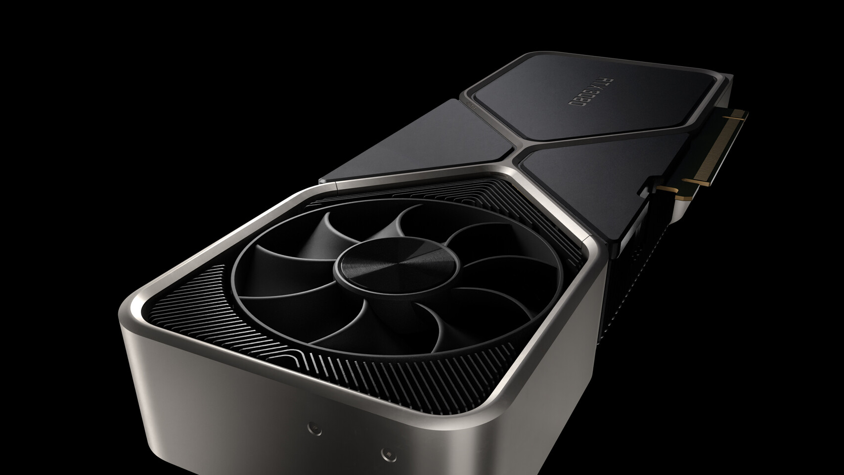
Possibly unsure of the GeForce RTX 3070 tackling AMD's Radeon RX 6000 series parts, NVIDIA is designing a new RTX 30-series SKU positioned between the RTX 3070 and RTX 3080. This is not a 16 GB variant of the RTX 3070, but rather a new SKU based on the 8 nm "GA102" silicon, according to a reliable source with NVIDIA leaks, kopite7kimi. The SKU is based on the GA102 with the ASIC code "GA102-150-KD-A1." The silicon is configured with 7,424 CUDA cores across 58 streaming multiprocessors (29 TPCs), 232 tensor cores, 232 TMUs, 58 RT cores, and an unknown number of ROPs. According to kopite7kimi, the card is configured with a 320-bit wide memory interface, although it's not known if this is conventional GDDR6, like the RTX 3070 has, or faster GDDR6X, like that on the RTX 3080.

NVIDIA recently "cancelled" a future 16 GB variant of the RTX 3070, and 20 GB variant of the RTX 3080, which is possibly the company calibrating its response to the Radeon RX 6000 series. We theorize that doubling in memory amounts may not have hit the desired cost-performance targets; and the company probably believes the competitive outlook of the RTX 3080 10 GB is secure. This explains the need for a SKU with performance halfway between that of the RTX 3070 and RTX 3080. As for pricing, with the RTX 3070 positioned at $500 and the RTX 3080 at $700, the new SKU could be priced somewhere in between. AMD's RDNA2-based Radeon RX 6000 series GPUs are expected to feature DirectX 12 Ultimate logo compliance, meaning that there is a level playing ground between AMD and NVIDIA in the performance segment.

Intel Partners with Heidelberg University Computing Center to Establish oneAPI Academic Center of Excellence

Intel and Heidelberg University Computing Center (URZ) today announced that they have established oneAPI Academic Center of Excellence (CoE) at UZR. The newly established CoE has a goal to further develop Intel's oneAPI standard and enable it to work on AMD GPUs. This information is a bit shocking, however, Intel believes that the technology should work on a wide range of processors, no matter the vendor. The heterogeneous hardware programming is the main goal here. In a Twitter thread, an Intel employee specifies that Intel has also been working with Arm and NVIDIA to bring Data-Parallel C++ (DPC++), a core of oneAPI, to those vendors as well. That should bring this universal programming model to every device and adapt to every platform, which is a goal of heterogeneous programming - whatever you need to program a CPU, GPU, or some other ASIC, it is covered by a single API, specifically oneAPI.
UZRURZ's work as a oneAPI CoE will add advanced DPC++ capabilities into hipSYCL, which supports systems based on AMD GPUs, NVIDIA GPUs, and CPUs. New DPC++ extensions are part of the SYCL 2020 provisional specification that brings features such as unified shared memory to hipSYCL and the platforms it supports - furthering the promise of oneAPI application support across system architectures and vendors.

NVIDIA GeForce RTX 3090 "CEO Edition" Rears its Head, Most Likely a Fake

Social media is abuzz with a screengrab of a regional webpage of the NVIDIA website purporting a "GeForce RTX 3090 CEO Edition" graphics card. Positioned a notch above the "Founders Edition," this $3,499 card, if even remotely real, could be a limited edition product. The screengrab references "48 GB of G6X" memory. We're not sure how this is even possible. The RTX 3090 already uses 8 Gbit GDDR6X chips, piggybacking two chips per 32-bit memory channel, unless Micron has done the unthinkable by launching a 16 Gbit G6X chip within 2020. Frankly, we're very interested to see how the next-gen Quadro RTX even achieves its alleged 48 GB of GDDR6.

That aside, the alloy frame now comes with a gold finish. We wonder if memory and a fancy trim is all that NVIDIA is asking the extra 2 Grand for, or if it even maxed out the "GA102" ASIC (there are two more TPCs left to unlock). As for the name "CEO Edition," there have been instances of tech CEOs flexing their vanity on limited edition products. Limited edition Ryzen and Radeon products, for example, bear the AMD CEO's signature. So the name "CEO Edition" by itself isn't implausible. Just not with these specs, and not this price.

Rambus Advances HBM2E Performance to 4.0 Gbps for AI/ML Training Applications

Rambus Inc. (NASDAQ: RMBS), a premier silicon IP and chip provider making data faster and safer, today announced it has achieved a record 4 Gbps performance with the Rambus HBM2E memory interface solution consisting of a fully-integrated PHY and controller. Paired with the industry's fastest HBM2E DRAM from SK hynix operating at 3.6 Gbps, the solution can deliver 460 GB/s of bandwidth from a single HBM2E device. This performance meets the terabyte-scale bandwidth needs of accelerators targeting the most demanding AI/ML training and high-performance computing (HPC) applications.

"With this achievement by Rambus, designers of AI and HPC systems can now implement systems using the world's fastest HBM2E DRAM running at 3.6 Gbps from SK hynix," said Uksong Kang, vice president of product planning at SK hynix. "In July, we announced full-scale mass-production of HBM2E for state-of-the-art computing applications demanding the highest bandwidth available."

Marvell Unveils the Industry's Most Comprehensive Custom ASIC Offering

Marvell today announced a unique custom ASIC offering that addresses the stringent requirements of next generation 5G carriers, cloud data centers, enterprise and automotive applications. Marvell's comprehensive custom ASIC solution enables a multitude of customization options and a differentiated approach with best-in-class standard product IP including Arm -based processors, embedded memories, high-speed SerDes, networking, security and a wide range of storage controller and accelerators in 5 nm and beyond. By partnering with Marvell, customers gain enhanced performance, power and area resulting in accelerated time-to-market and providing optimal returns on investment.

Traditionally, data infrastructure manufacturers and cloud data center operators have had to choose between securing standard products or a full custom silicon solution designed in-house, while developing or licensing foundational IP as needed. Now, for the first time, Marvell is offering full access to its broad and growing portfolio of industry-leading data infrastructure standard product IP and technologies, which can be integrated and enabled in custom ASIC solutions at the most advanced technology nodes.

AMD RDNA2 "Navi 21" GPU to Double CU Count Over "Navi 10"

AMD's RDNA2 graphics architecture, which sees real-time ray-tracing among other DirectX 12 Ultimate features, could see the company double the amount of stream processors generation-over-generation, according to a specs leak by _rogame. The increase in stream processors would fall in line with AMD's effort to increase performance/Watt by 50%. It may appear like the resulting SKUs finally measure up to the likes of the RTX 2080 Ti, but AMD has GeForce "Ampere" in its competitive calculus, and should the recent specs reveal hold up, the new "Navi 21" could end up being a performance-segment competitor to GeForce graphics cards based on the "GA104" ("TU104" successor), rather than a flagship-killer.

The RDNA2-based "Navi 21" GPU allegedly features 80 RDNA2 compute units amounting to 5,120 stream processors. AMD might tap into a refined 7 nm-class silicon fabrication node by TSMC to build these chips, either N7P or N7+. The die-size could measure up to 505 mm², and AMD could aim for a 50% performance/Watt gain over the "Navi 10." AMD could carve out as many as 10 SKUs out of the "Navi 21," but only three are relevant to the gamers. The SKU with the PCI device ID "0x731F: D1" succeeds the RX 5700 XT. The one bearing "0x731F: D3" succeeds the RX 5700, with a variant name "Navi 21 XL." The "Navi 21 XE" variant has a PCI ID of "0x731F: DF," and succeeds the RX 5600 XT.

Vicor 1200A Hydra ChiP-set Enables Higher Performance AI Accelerator Cards

Vicor Corporation today announced a ChiP-set for high performance GPU, CPU, and ASIC ("XPU") processors powered directly from 48 V. A driver, MCD4609, and a pair of MCM4609 current multiplier modules supply up to 650 A continuous and 1200 A peak. Owing to their small footprint and low profile (45.7 x 8.6 x 3.2 mm), current multipliers are placed close to the processor enabling reduced power distribution network (PDN) losses and higher power system efficiency. Powering GPU and OCP Accelerator Module (OAM) Artificial Intelligent (AI) cards, the 4609 ChiP-set is in mass production and available to new customers on the Vicor Hydra II evaluation board.

The 4609 ChiP-set adds to the Vicor Power-on-Package portfolio of Lateral Power Delivery (LPD) solutions. To raise the bar of current capability above the limits of LPD, Vicor's pioneering Vertical Power Delivery (VPD) will soon enable much higher current density. The VPD system delivers current from power converters vertically stacked under a processor through a capacitor network geared to a processor-specific pin-map. A GCM ("Gearbox Current Multiplier") is a specialized VPD embodiment incorporating a gearbox capacitor network as a layer in the vertical stack. By supplying current directly under the processor and eliminating PDN losses, GCMs will soon facilitate current densities reaching up to 2 A per mm².

Intel Reports First-Quarter 2020 Financial Results

Intel Corporation today reported first-quarter 2020 financial results. "Our first-quarter performance is a testament to our team's focus on safeguarding employees, supporting our supply chain partners and delivering for our customers during this unprecedented challenge," said Bob Swan, Intel CEO."The role technology plays in the world is more essential now than it has ever been, and our opportunity to enrich lives and enable our customers' success has never been more vital. Guided by our cultural values, competitive advantages and financial strength, I am confident we will emerge from this situation an even stronger company."

In the first quarter, Intel achieved 34 percent data-centric revenue growth and 14 percent PC-centric revenue growth YoY. The company maintained essential factory operations with greater than 90 percent on-time delivery while supporting employees, customers and communities in response to the COVID-19 pandemic. This includes a new Intel Pandemic Response Technology Initiative to combat the virus where we can uniquely make a difference with Intel technology, expertise, and resources.

TSMC and Broadcom Enhance the CoWoS Platform with World's First 2X Reticle Size Interposer

TSMC today announced it has collaborated with Broadcom on enhancing the Chip-on-Wafer-on-Substrate (CoWoS ) platform to support the industry's first and largest 2X reticle size interposer. With an area of approximately 1,700mm2, this next generation CoWoS interposer technology significantly boosts computing power for advanced HPC systems by supporting more SoCs as well as being ready to support TSMC's next-generation five-nanometer (N5) process technology.

This new generation CoWoS technology can accommodate multiple logic system-on-chip (SoC) dies, and up to 6 cubes of high-bandwidth memory (HBM), offering as much as 96 GB of memory. It also provides bandwidth of up to 2.7 terabytes per second, 2.7 times faster than TSMC's previously offered CoWoS solution in 2016. With higher memory capacity and bandwidth, this CoWoS solution is well-suited for memory-intensive workloads such as deep learning, as well as workloads for 5G networking, power-efficient datacenters, and more. In addition to offering additional area to increase compute, I/O, and HBM integration, this enhanced CoWoS technology provides greater design flexibility and yield for complex ASIC designs in advanced process nodes.

Rambus Achieves Industry-Leading GDDR6 Performance at 18 Gbps

Rambus Inc., a premier silicon IP and chip provider making data faster and safer, today announced it has achieved industry-leading 18 Gbps performance with the Rambus GDDR6 Memory PHY. Running at the industry's fastest data rate of 18 Gbps, the Rambus GDDR6 PHY IP delivers peak performance four-to-five times faster than current DDR4 solutions and continues the company's longstanding tradition of developing leading-edge products. The Rambus GDDR6 PHY pairs with the companion GDDR6 memory controller from the recent acquisition of Northwest Logic to provide a complete and optimized memory subsystem solution.

Increased data usage in applications such as AI, ML, data center, networking and automotive systems is driving a need for higher bandwidth memory. The coming introduction of high-bandwidth 5G networks will exacerbate this challenge. Working closely with our memory partners, the Rambus GDDR6 solution gives system designers more options in selecting the memory system that meets both their bandwidth and cost requirements.
Return to Keyword Browsing
Apr 25th, 2024 00:49 EDT change timezone

New Forum Posts

Popular Reviews

Controversial News Posts