News Posts matching #CUDA

Return to Keyword Browsing

NVIDIA GPUs Power Top Two Russian Supercomputers

NVIDIA today announced that the two most powerful supercomputers in Russia will use NVIDIA GPUs to address some of the world's most challenging scientific problems across a broad range of fields.

Underscoring the dramatic growth in the adoption of GPU computing across world scientific communities, the new Russia Top 50 supercomputer list released today reveals that the top two systems are accelerated by NVIDIA Tesla GPUs. These two supercomputers are housed at Lomonosov Moscow State University, which was recently named a CUDA Center of Excellence, and the Joint Supercomputer Center of the Russian Academy of Sciences (JSCC RAS). Moreover, GPUs are accelerating 12 of the country's top 50 systems -- up from seven just six months ago.

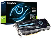
GIGABYTE Out With its GeForce GTX 680

GIGABYTE took its own sweet time launching its GeForce GTX 680, but no harm done. Carrying the product code GV-N680D5-2GD-B, GIGABYTE's graphics card sticks to NVIDIA reference board design, decorated with a slick-looking abstract art. The card also sticks to NVIDIA reference clock speeds of 1006 MHz (core), 1058 MHz (boost), and 1502 MHz / 6.00 GHz effective GDDR5 memory. It is armed with 2 GB of memory sitting across a 256-bit wide memory interface. Based on the 28 nm GK104 GPU, NVIDIA GeForce GTX 680 is powered by 1536 CUDA cores, and a revolutionary, energy-efficient architecture. GIGABYTE GeForce GTX 680 is priced at US $499.

Galaxy GeForce GTX 680 Launched

One of NVIDIA's biggest board partners by volume, Galaxy unveiled its GeForce GTX 680. Its lineup has just the one model as of today, which sticks to NVIDIA reference board and cooler designs, with minor aesthetic touches. Galaxy's card also sticks to NVIDIA reference clock speeds of 1006/1056/6000 MHz (core/boost/memory effective). The 28 nm chip packs 1536 CUDA cores, and a 256-bit wide memory interface, holding 2 GB of memory. Galaxy's card is priced at US $499.

NVIDIA Launches the GeForce GTX 680 "Kepler" Graphics Card

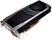
NVIDIA today launched the first model in the GeForce Kepler GPU family, the GeForce GTX 680. Based on the spanking new "Kepler" architecture, and a high-performance chip derived from it, GK104, and built on the 28 nm fab process at TSMC, the GeForce GTX 680 is NVIDIA's fresh bid for single-GPU performance supremacy. The new chip packs a staggering 1536 CUDA cores (three-fold increase over GTX 580), 2 GB of GDDR5 memory over a 256-bit wide memory interface, and staggering clock speeds of 1006 MHz (core base), 1056 MHz (core boost), and 1502 MHz (memory, 6.00 GHz effective), with a memory interface bandwidth of 192 GB/s.

It doesn't stop there. NVIDIA introduced a clever new technology called GPU Boost, which makes the GPU self-aware of parameters such as load, voltages, temperatures, and auto-tunes clock speeds, to deliver the best performance per Watt ratio. NVIDIA also introduced Adaptive V-Sync, which smooths transition between lower than refresh-rate frame-rates, and V-sync rate, attempting to eliminate lag, and naturally prevent page-tearing. NVIDIA also introduced the new TXAA anti-aliasing algorithm, which is a performance-efficient image quality enhancement. To top it all off, the chip has a TDP of just 195W. Available today, though leading retailers in mature markets, the NVIDIA GeForce GTX 680 is priced at US $499 (MSRP).

GK110 Specifications Approximated

Even as launch of the GK104-based GeForce GTX 680 nears, it's clear that it is emerging that it is not the fastest graphics processor in the GeForce Kepler family, if you sift through the specifications of the GK110 (yes, 110, not 100). Apparently, since GK104 meets or even exceeds the performance expectations of NVIDIA, the large-monolithic chip planned for this series, is likely codenamed GK110, and it's possible that it could get a GeForce GTX 700 series label.

3DCenter.org approximated the die size of the GK110 to be around 550 mm², 87% larger than that of the GK104. Since the chip is based on the 28 nm fab process, this also translates to a large increment in transistor count, up to 6 billion. The shader compute power is up by just around 30%, because the CUDA core count isn't a large increment (2000~2500 cores). The SMX (streaming multiprocessor 10) design could also face some changes. NVIDIA could prioritize beefing up other components than the CUDA cores, which could result in things such as a 512-bit wide GDDR5 memory interface. The maximum power consumption is estimated to be around 250~300 Watts. Its launch cannot be expected before August, 2012.

Inno3D GeForce GTX 560 SE Pictured

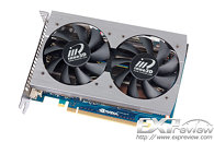
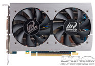
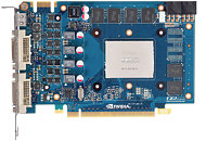
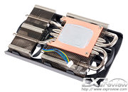
Here are some of the first pictures of Inno3D GeForce GTX 560 SE. Inno3D implemented NVIDIA's new SKU that's competitive with Radeon HD 7700 series, by designing a compact graphics card that's backed by relatively-powerful cooling. The PCB is very short (good for compact cases), and uses a simple 4+1 phase VRM to power the card. It features 1 GB of GDDR5 memory sitting on a 192-bit wide memory interface. The GTX 560 SE packs 288 CUDA cores, and clock speeds of 776/1553/953 MHz (core/CUDA cores/memory actual). Inno3D GeForce GTX 560 SE is cooled by a custom dual-slot cooling solution. This cooler makes use of two aluminum fin stacks, to which heat is conveyed by four 8 mm-thick nickel-plated copper heat pipes. The fin stacks are then ventilated by two 80 mm fans. The card has been tested at the source.

New Acer Aspire Timeline M3 Packs GeForce GT 640M, Too

NVIDIA seems to have scored big design wins with Acer, for its next-generation GPUs. First, we had reports of Acer's VA40 combining Intel "Ivy Bridge" Core processors with NVIDIA GeForce GT 640M, and now Acer Timeline M3-581TG, following the same path. The M3-581TG is a 15.6-inch Ultrabook (one of the first of its kind). Pictures of this model reveal case-badges of its key components, including an NVIDIA GEFORCE GT case-badge, which gives out GPU model (GeForce GT 640M) and memory amount (1 GB). This could very well be the way NVIDIA's GeForce GT family of GPUs will be designated in case-badges.

Based on the 28 nm GK107 silicon, the GeForce GT 640M packs 384 CUDA cores running at speeds of up to 625 MHz, with 405 MHz base clock, and 910 MHz DDR3 memory, churning up 28.8 GB/s memory bandwidth. Other notable components of the Timeline M3-581TG include Intel Core i7-2637M (1.7 GHz dual-core, 4 MB of L3 cache) processor, 4 GB DDR3-1333 memory, and 256 GB SSD.

GeForce GTX 680 Specifications Sheet Leaked

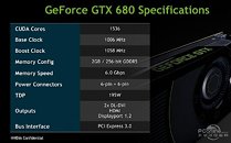
Chinese media site PCOnline.com.cn released what it claims to be an except from the press-deck of NVIDIA's GeForce GTX 680 launch, reportedly scheduled for March 22. The specs sheet is in tune with a lot of information that we already came across on the internet, when preparing our older reports. To begin with the GeForce GTX 680 features clock speeds of 1006 MHz (base), and 1058 MHz (boost). The memory is clocked at a stellar 6.00 GHz (1500 MHz actual), with a memory bus width of 256-bit, it should churn out memory bandwidth of 192 GB/s. 2 GB is the standard memory amount.

For the umpteenth time, this GPU does feature 1,536 CUDA cores. The card draws power from two 6-pin PCIe power connectors. The GPU's TDP is rated at 195W. Display outputs include two DVI, and one each of HDMI and DisplayPort. Like with the new-generation GPUs from AMD, it supports PCI-Express 3.0 x16 bus interface, which could particularly benefit Ivy Bridge and Sandy Bridge-E systems, in cases where the link width is reduced to PCI-Express 3.0 x8 when there are multiple graphics cards installed.

GK104 Dynamic Clock Adjustment Detailed

With its GeForce Kepler family, at least the higher-end parts, NVIDIA will introduce what it calls Dynamic Clock Adjustment, which adjusts the clock speeds of the GPU below, and above the base-line clock speeds, depending on the load. The approach to this would be similar to how CPU vendors do it (Intel Turbo Boost and AMD Turbo Core). Turning down clock speeds under low loads is not new to discrete GPUs, however, going above the base-line dynamically, is.

There is quite some confusion regarding NVIDIA continuing to use "hot clocks" with GK104, the theory for and against the notion have been enforced by conflicting reports, however we now know that punters with both views were looking at it from a binary viewpoint. The new Dynamic Clock Adjustment is similar and complementary to "hot clocks", but differs in that Kepler GPUs come with a large number of power plans (dozens), and operate taking into account load, temperature, and power consumption.

NVIDIA Tesla GPUs Accelerate Science on HP ProLiant Generation 8 Servers

NVIDIA today announced that its NVIDIA Tesla GPUs will be included in HP ProLiant Generation 8 (Gen8) servers, delivering new levels of computational performance for scientific applications at world-class power efficiency.

HP ProLiant SL250 Gen8 CPU-GPU hybrid servers combine the world's most powerful parallel processors, NVIDIA Tesla M2090 GPUs, with new Intel Xeon E5-2600 series CPUs based on the Sandy Bridge microarchitecture.

GeForce GTX 680 Features Speed Boost, Arrives This Month, etc., etc.

Here are some key bits of information concerning the upcoming GeForce GTX 680, a performance single-GPU graphics card based on the 28 nm GK104 GPU by NVIDIA. The information, at face value, is credible, because we're hearing that a large contingent of the media that finds interest in the GPU industry, is attending the Game Developers Conference, where it could interact with NVIDIA, on the sidelines. The source, however, is citing people it spoke to at CeBIT.

First, and most interesting: with some models of the GeForce 600, NVIDIA will introduce a load-based clock speed-boost feature (think: Intel Turbo Boost), which steps up clock speeds of the graphics card when subjected to heavy loads. If there's a particularly stressing 3D scene for the GPU to render, it overclocks itself, and sees the scene through. This ensures higher minimum and average frame-rates.

NVIDIA GPUs Bring High Performance GPU Computing To New Dell PowerEdge Servers

NVIDIA today announced that its NVIDIA Tesla GPUs will be featured, for the first time, on two Dell PowerEdge 12th generation rack and tower servers.

Dell designed the new GPU-enabled PowerEdge R720 and PowerEdge T620 servers to accelerate a wide range of computationally intensive, industry standard applications, including Mathworks MATLAB (for computational research) and SIMULIA Abaqus (for computer-aided engineering). In addition, the new servers combine the 512-core NVIDIA Tesla M2090 GPUs with the latest Intel Xeon E5/R CPUs based on the Sandy Bridge microarchitecture to accelerate a range of scientific applications in fields such as life sciences, engineering, weather and climate, and others.

Battle-Ready MSI GT685 Gaming Laptop Comes to Thailand

MSI is rolling out its new generation GT685-the ultimate gaming machine. In addition to featuring the Intel second generation Core i7 quad core processor, it is the first laptop to sport the nVidia GeForce GTX 580M, the world's fastest discrete graphics card, 32G DDR3 of memory, and accelerated dual hard disk architecture. It comes with Dynaudio and THX TruStudio Pro smart wrap around sound as well as a full HD screen. The MSI GT685 was awarded Editor's Choice by Thai IT mag Notebook4game.com and to ensure that it remains the top-selling gaming NB brand in Thailand, MSI is holding activities on university campuses to give gaming enthusiasts the opportunity to experience its gaming laptops.

23 Universities and Institutions Added As NVIDIA CUDA Research/Teaching Centers

Today, NVIDIA welcomes 23 universities and research institutions to its family of CUDA Research Centers and CUDA Teaching Centers.

CUDA Teaching Centers empower tens-of-thousands of students each year with the knowledge and expertise to take advantage of GPUs and their parallel-processing capabilities. These centers receive teaching kits, textbooks, software licenses and NVIDIA CUDA architecture-enabled GPUs for teaching lab computers, as well as academic discounts for additional hardware.

NVIDIA Prepares GeForce GTX 560 SE to Thwart Radeon HD 7770

For an immediate relief from the market-threat looming in the sub-$200 segment with the introduction of AMD's Radeon HD 7770, NVIDIA is planning to carve out a new SKU based on the 40 nm GF114 GPU, the GeForce GTX 560 SE. The new SKU will be positioned below the GeForce GTX 560 (non-Ti), and target price-points well within $200. The new SKU is identical to the OEM-only model GeForce GTX 555. Its specifications follow:
  • Based on 40 nm GF114 ASIC
  • 288 CUDA cores
  • 48 TMUs, 24 ROPs
  • 192-bit wide GDDR5 memory interface
  • 1 GB standard memory amount (asymmetric memory chip arrangement à la GTX 550 Ti)
  • Clock speeds: 776 MHz core; 1553 MHz CUDA cores; 952 MHz (3.828 GHz effective) memory, 92 GB/s memory bandwidth

New Lesance Type-GX Reference Configuration Packs GeForce GT 630M Graphics

Japanese build-to-order PC specialists Lesance launched the BTO GSN721GW TYPE-GX reference 17-inch performance notebook featuring NVIDIA GeForce GT 630M graphics. At 17-inches size, the Type-GX serves as a portable desktop-replacement. Its screen packs full-HD resolution (1920 x 1080), the GeForce GT 630 driving it is backed by 1 GB of DDR3 memory. It packs 144 CUDA cores.

Other parts of the Type-GX include Intel Core i7-2670QM quad-core processor clocked at 2.20 GHz with 6 MB L3 cache, 8 GB (4 GB x2, DDR3-1333 SO-DIMM) memory, Intel 510 Series 120 GB SSD, Blu-ray ROM, wireless b/g/n and gigabit Ethernet connections, and USB 3.0 ports. The notebook measures 416 x 270 x 22 ~ 35 mm (WxDxH), weighing 2.99 kg. Windows 7 Home Premium x64 is the OS of choice. This reference configuration costs 101,980 JPY (US $1320).

NVIDIA Releases CUDA Toolkit 4.1

NVIDIA today released a new version of its CUDA parallel computing platform, which will make it easier for computational biologists, chemists, physicists, geophysicists, other researchers, and engineers to advance their simulations and computational work by using GPUs.

The new NVIDIA CUDA parallel computing platform features three key enhancements that make parallel programing with GPUs easier, more accessible and faster. These include:

- Re-designed Visual Profiler with automated performance analysis, providing an easier path to application acceleration
- New compiler, based on the widely-used LLVM open-source compiler infrastructure, delivering up to 10 percent speed up in application performance
- Hundreds of new imaging and signal processing functions, doubling the size of the NVIDIA Performance Primitives (NPP) library

NVIDIA Opens Up CUDA Platform by Releasing Compiler Source Code

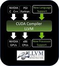
NVIDIA today announced that it will provide the source code for the new NVIDIA CUDA LLVM-based compiler to academic researchers and software-tool vendors, enabling them to more easily add GPU support for more programming languages and support CUDA applications on alternative processor architectures.

LLVM is a widely-used open source compiler infrastructure with a modular design that makes it easy to add support for new programming languages and processor architectures. It is used for a range of programming requirements by many leading companies, including Adobe, Apple, Cray, Electronic Arts, and others.

GeForce Kepler 104 and 100 GPU Specifications Compiled

A quick stroll through our previous article about how the GeForce Kepler family of next-generation GPUs is laid out, would tell you that GeForce Kepler 104 (GK104), is going to be NVIDIA's answer to AMD's Tahiti. GK104 will be a high-performance (≠ high-end) GPU by NVIDIA that will have many of the features that were reserved for its previous high-end GPUs (such as a 384-bit wide GDDR5 memory interface), but will not be NVIDIA's most powerful GPU in the series. The throne will be kept empty for GK100, which will comply with NVIDIA's "go all in" design ideology for high-end GPUs.

3DCenter.org compiled a few specifications of the GK104 and GK100. They go like this:
GK104
  • 640 to 768 CUDA cores
  • 80 to 96 TMUs (depending on what the CUDA core count ends up being)
  • 384-bit GDDR5 memory interface, 48 ROPs
  • Built on the 28 nm TSMC process
  • Products based on this will launch in the first quarter of 2012

Club 3D Announces GeForce GTX 560 Ti CoolStream with 2 GB Memory

Club 3D announced its newest performance-segment graphics card, the GTX 560 Ti CoolStream with 2 GB of GDDR5 memory (model: CGNX-XT5648). Based on the 40 nm GF-114 silicon, this card features 384 CUDA cores, and makes use of 2 GB of GDDR5 memory, double the standard memory amount, across a 256-bit wide memory interface. It sports a compact in-house PCB design by Club 3D, and is cooled by an in-house dual-fan cooling solution that makes use of heat pipes to convey heat through stacks of aluminum fins, which are then ventilated by two 80 mm fans.

The card features clock speeds of 822 MHz core, 1644 MHz CUDA cores, and 1002 MHz (4008 MHz effective) memory, sticking to NVIDIA reference speeds. The card is 2-way SLI capable, draws power from two 6-pin PCIe power connectors, and its display outputs include two DVI and a mini-HDMI. The new Club 3D GeForce GTX 560 Ti CoolStream 2 GB is expected to be priced at €245 or US $329, including taxes. Club 3D will also launch a special edition of this card that includes a license of Battlefield 3. The Battlefield 3 Edition variant will be priced at €265 or $355, including taxes.

GIGABYTE Intros GeForce GTX 560 Ti 448 Cores Windforce Graphics Card

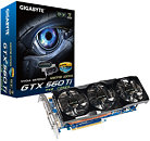
GIGABYTE unveiled its GeForce GTX 560 Ti 448 Cores graphics card offering, the GV-N560448-13I. This card is based on Gigabyte's in-house GF110 Ultra Durable VGA PCB, and is cooled by its own Windforce 3X Vapor-Chamber cooler. The card sticks to NVIDIA reference clock speeds of 732/1464/950(3800) MHz core/CUDA cores/memory(effective). It packs 448 CUDA cores, and 1280 MB of memory across a 320-bit wide GDDR5 memory interface.

The Ultra Durable VGA PCB makes use of a 2 oz copper layer to improve cooling and electrical stability, ferrite core chokes, Japanese solid-state capacitors, low RDS (on) MOSFETs, and tier-1 Samsung GDDR5 memory chips. The Windforce 3X Vapor-Chamber cooler makes use of a large vapor-chamber base from which heat is conveyed to aluminum fin stacks. These are ventilated by three outward-inclined 80 mm fans. Like every other GeForce GTX 560 Ti 448 Cores, this card will be available in limited quantities, in the US, Canada, UK, Germany, France, Russia, and the Nordics. It will be priced under US $300.

NVIDIA GeForce GTX 560 Ti with 448 Cores Launched

NVIDIA released its newest graphics card model specifically for the winter shopping season, the limited edition GeForce GTX 560 Ti 448 cores. Not only is this a limited edition launch, but also targeting only specific markets in North America and Europe. This includes the United States and Canada in North America; and the UK, France, Germany, Russia, and the Nordics in Europe. The new card is based on the 40 nanometer GF110 GPU instead of the GF114 that the regular GTX 560 Ti is based on. This allows NVIDIA to add 64 more CUDA cores (448 vs. 384), 25% more memory (1280 MB vs. 1024), and a 25% wider memory bus (320 bit vs. 256).

The new limited edition GeForce GTX 560 Ti 448 cores features clock speeds identical to those on the GeForce GTX 570, at 732 MHz core, 1464 MHz CUDA cores, and 950 MHz (3.80 GHz effective) GDDR5 memory. Since it's based on the GF110 board, this new card is also capable of 3-way SLI, something the regular GTX 560 Ti isn't. The card draws power from two 6-pin PCIe power connectors. Display outputs typically include two DVI and a mini-HDMI. Add-in card vendors are free to design their own graphics cards based on this chip, and so expect most GTX 560 Ti 448 core cards to look similar to non-reference GTX 570 ones. ZOTAC, Inno3D, EVGA, Palit, Gainward, ASUS, Gigabyte, and MSI will have graphics cards based on this chip. Prices should typically start at US $289.

TechPowerUp GPU-Z v0.5.6 Released

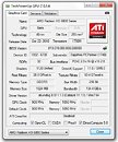
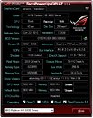
TechPowerUp released a new version of GPU-Z, version 0.5.6. GPU-Z is our popular graphics card information and diagnostic utility that gives you technical details of the graphics hardware installed in your PC, and lets you monitor fine details such as clock speeds, temperatures, and voltages. The new version adds preliminary support for some of NVIDIA's upcoming GeForce Kepler family GPUs. It also adds support for NVIDIA GeForce GTX 560 Ti 448 CUDA cores, which will be launched this 29th. Support is also added for AMD Radeon HD 6320, FirePro V9800, FirePro V4900, GeForce GTX 460 V2 (GTX 460 based on GF114), Quadro NVS 420, Quadro NVS 450, and Quadro FX 380 LP. A small bug related to incorrect shader reading on "Blackcomb" is fixed.

DOWNLOAD: TechPowerUp GPU-Z 0.5.6 | GPU-Z 0.5.6 ASUS ROG Edition

Galaxy GeForce GTX 550 Ti Display4 Graphics Card Pictured

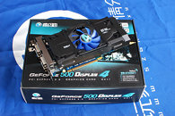
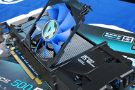
Here are the first pictures of Galaxy's GeForce GTX 550 Ti Display4 graphics card, designed exclusively for Asian markets. As its name might suggest, it is a GeForce GTX 550 Ti based graphics card designed to support up to four displays. The card uses an IDT VMM 1403 display output logic chip that lets it effectively make use of the total resolution the GPU supports. The redesigned display logic supports a total resolution of 5760 x 1080. Spread across four displays, you get 1440 x 1080 per display, or spread it across three displays to get 1920 x 1080 per display. Apart from four DVI connectors, its output logic makes room for a mini-HDMI connector.

The GeForce GTX 550 Ti is aided by 1 GB of GDDR5 memory across a 192-bit wide memory interface. It is powered by a 3+1 phase VRM controlled by Galaxy's in-house G-Engine chip. The GTX 550 Ti packs 192 CUDA cores, and clock speeds of 950 MHz core, 1900 MHz CUDA cores, and 1025 MHz (4.10 GHz effective) GDDR5 memory. Galaxy also used its in-house "Glaciator" cooler, which makes use of a heat-pipe fed heatsink ventilated by a large central fan. This can can be partially detached to help clean it, and the portion of the heatsink directly underneath it. Galaxy's GTX 550 Ti Display4 is priced at RMB 999 (converts to US $157).

NVIDIA Tesla GPUs Again Power World's Greenest Petaflop Supercomputer

NVIDIA today announced that, for the second year in a row, the world's most energy efficient petaflop-class supercomputer is powered by NVIDIA Tesla GPUs.

The Tsubame 2.0 system at the Tokyo Institute of Technology's Global Scientific Information Center (GSIC) ranks as the greenest petaflop-class supercomputer on the recently released Green500 list. Published twice annually, the Green500 list, rates the 500 most energy efficient supercomputers based on performance achieved relative to power consumed.

Tsubame 2.0 is a heterogeneous supercomputer (combining both CPUs and GPUs) used to accelerate a range of scientific and industrial research in Japan. With sustained performance of 1.19 petaflops per second while consuming 1.2 megawatts, Tsubame 2.0 delivers 958 megaflops of processing power per watt of energy. It is 3.4-times more energy efficient than the next-closest x86 CPU-only petaflop system, the Cielo Cray supercomputer at Los Alamos National Laboratory, which delivers 278 megaflops per watt.
Return to Keyword Browsing
Apr 23rd, 2024 08:54 EDT change timezone

New Forum Posts

Popular Reviews

Controversial News Posts