News Posts matching #Cache

Return to Keyword Browsing

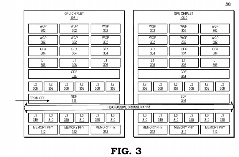
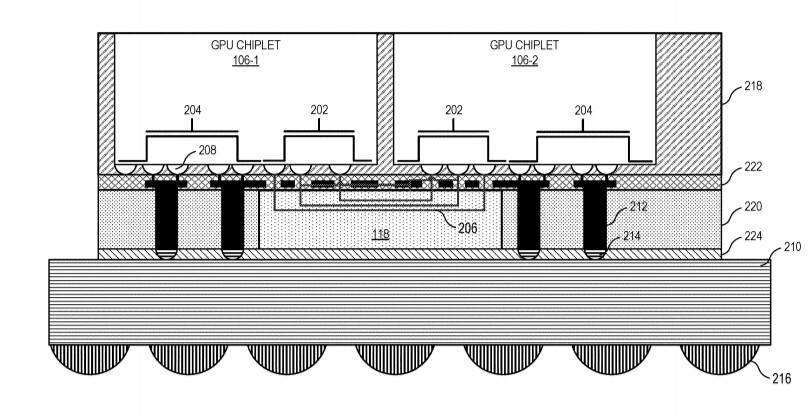
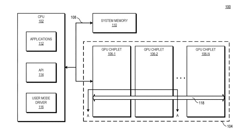
MSI Announces the SPATIUM M580 FROZR: A Groundbreaking PCIe Gen 5 SSD Redefining Speed and Reliability

MSI, a global leader in gaming PC hardware, is thrilled to announce the release of its highly anticipated SSD powerhouse, the SPATIUM M580 FROZR, ushering in a new era of storage performance. With cutting-edge technology and innovative thermal solutions, this SSD is set to redefine the standards of speed and reliability in storage solutions.

SPATIUM M580 FROZR, Reaching New Heights with Crowned Speeds
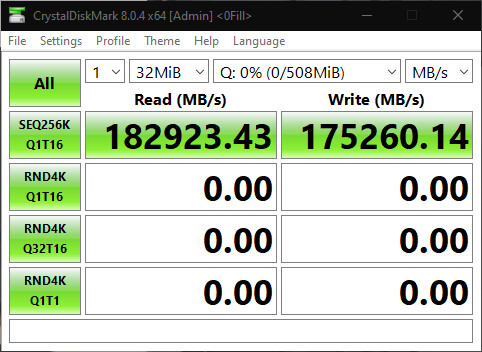
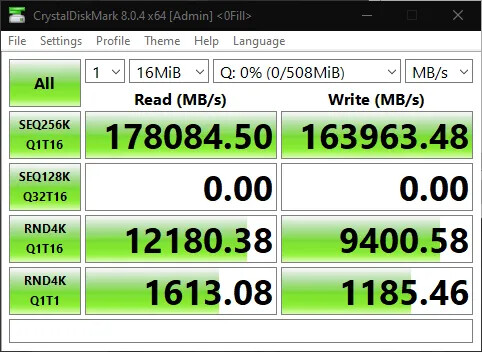
The SPATIUM M580 FROZR sets a new benchmark in storage performance with its revolutionary features. Powered by the state-of-the-art PHISON E26 PCIe Gen 5 controller and equipped with advanced 3D NAND flash modules boasting 232 layers, this SSD achieves mind-blowing read speeds of up to 14.6 GB/s and write speeds of up to 12.7 GB/s, up to 2 times faster transfer rates compared to current PCIe 4.0 SSDs. This represents a significant leap in speeds, boosted by a DRAM cache buffer and a SLC Cache, providing users with lightning-fast data access and gaining valuable milliseconds in latency for gaming, content creation, and professional applications. Additionally, the M580 FROZR is fortified with LPDC ECC and E2E Data Protection, ensuring data integrity and reliability. With a high TBW (Terabytes Written) value and backed by a comprehensive 5-year warranty, users can trust in the durability and longevity of the SPATIUM M580 FROZR in 1 TB, 2 TB and 4 TB variants after an easy installation.

Intel Xeon W9-3595X Spotted with 60 Cores, 112 MB of L3 Cache, and 4.60 GHz Frequency

Intel's upcoming high-end desktop (HEDT) processor lineup for enthusiasts and prosumers is around the corner, and today, we managed to see the flagship SKU - the Xeon W9-3595X. Spotted recently on Geekbench benchmarks, this new chip packs a whopping 60 cores and 120 threads, making it Intel's highest core count HEDT offering yet. The Xeon W9-3595X is based on Intel's advanced Sapphire Rapids architecture, built using the Intel 7 process node. It succeeds the previous flagship 56-core W9-3495X, with four additional cores crammed into the new 350 Watt TDP envelope. Clock speeds have taken a slight hit to accommodate the extra cores, with the maximum turbo frequency lowered from 4.8 GHz on the 3495X to 4.6 GHz on the new 3595X.

However, with more cores, the 3595X should still offer a significant multi-threaded performance uplift for heavily parallel workloads. The Xeon W9-3595X will drop into existing LGA-4677 motherboards, like the ASUS PRO WS 790-ACE, after a BIOS update. It features 112 MB of L3 cache, 120 MB of L2 cache (2 MB per core), and continues Intel's push towards higher core counts for enthusiasts, content creators, and workstation users who need maximum multi-threaded horsepower. Pricing and availability details remain unannounced as of now. But with an appearance on public databases, an official launch of the 60-core HEDT juggernaut seems imminent. These new Sapphire Rapids SKUs will likely have extra AI features, like dedicated AI acceleration engines, in the same manner that server-class SKUs do.

NVIDIA Corrects L2 Cache Spec for GeForce RTX 4070 SUPER

NVIDIA has recently revised its specification sheet for the upcoming GeForce RTX 4070 SUPER GPU—a small mistake was included in their review guide and marketing material. Team Green workers were likely in a rush to get everything ready for RTX 40xx SUPER range's official unveiling at CES 2024, so a typo here and there is not unexpected. The RTX 4070 SUPER's AD104 GPU configuration was advertised as offering a 20% core count upgrade over the vanilla RTX 4070 (non-SUPER), but detail sensitive sleuths were somewhat puzzled with the SUPER's L2 cache designation of 36 MB. Various 2023 leaks suggested that 48 MB was the correct value; representing a 33% jump up from the standard 4070's L2 pool. We must note that TPU's GPU database had the correct spec entry since day one.

AMD 3D V-Cache RAM Disk Delivers Over 182 GB/s and 175 GB/s Read and Write Speeds

AMD's 3D V-Cache technology utilizes blocks of SRAM stacked on top of the CPU logic die, where CPU cores reside, and allows the processor to access massive pools of cache for applications. However, using this extra level 3 (L3) cache as a RAM disk appears possible, where the L3 SRAM behaves similarly to a storage drive. A big disclaimer here is that this is only possible by exposing the L3 to the CrystalDiskMark benchmark, and no real-world applications can do it in a way that CrystalDiskMark. According to X/Twitter user Nemez (@GPUsAreMagic), the steps to replicate this procedure are: Obtaining an AMD Ryzen CPU with 3D V-Cache, installing OSFMount and creating a FAT32 formatted RAM disk, and running CrystalDiskMark, with values set to values to SEQ 256 KB, Queue Depth 1, Threads 16, and data fill to 0s instead of random.

The results of this experiment? Well, they appear to be rather stunning as the nature of L3 SRAM is that the memory is tiny but very fast and accessible to the CPU, so it can help load data locally before going to the system RAM. With AMD Ryzen 7 5800X3D, the speeds of this RAM disk are over 182 GB/s for reading and over 175 GB/s for writing. In another test, shared by Albert Thomas (@ultrawide219), we managed to see RAM disk based on AMD Ryzen 7800X3D V-Cache, which scores a little less with over 178 GB/s read and over 163 GB/s write speeds. Again, CrystalDiskMark only performed these tests on small allocations varying between 16 MiB and 32 MiB, so no real-world workloads are yet able to utilize this.

TYAN Announces New Server Line-Up Powered by 4th Gen AMD EPYC (9004/8004 Series) and AMD Ryzen (7000 Series) Processors at SC23

TYAN, an industry leader in server platform design and a subsidiary of MiTAC Computing Technology Corporation, debuts its new server line-up for 4th Gen AMD EPYC & AMD Ryzen Processors at SC23, Booth #1917, in the Colorado Convention Center, Denver, CO, November 13-16.

AMD EPYC 9004 processor features leadership performance and is optimized for a wide range of HPC, cloud-native computing and Generative AI workloads
TYAN offers server platforms supporting the AMD EPYC 9004 processors that provide up to 128 Zen 4C cores and 256 MB of L3 Cache for dynamic cloud-native applications with high performance, density, energy efficiency, and compatibility.

Intel Arrow Lake-S to Feature 3 MB of L2 Cache per Performance Core

Intel's next-generation designs are nearing launch, and we are already getting information about the upcoming generations. Today, we have the information that Intel's Arrow Lake-S desktop/client implementations of the Arrow Lake family will feature as much as 3 MB of level two (L2) cache for each performance core. Currently, Intel's latest 13th-generation Raptor Lake and 14th-generation Raptor Lake Refresh feature 2 MB of L2 cache per performance core. However, the 15th generation Arrow Lake, scheduled for launch in 2024, will bump that up by 50% and reach 3 MB. Given that P-cores are getting a boost in capacity, we expect E-cores to do so as well, but at a smaller size.

Arrow Lake will utilize Lion Cove P-core microarchitecture, while the E-core design will be based on Skymont. Intel plans to use a 20A node for this CPU, and more details will be presented next year.

NVIDIA Explains GeForce RTX 40 Series VRAM Functionality

NVIDIA receives a lot of questions about graphics memory, also known as the frame buffer, video memory, or "VRAM", and so with the unveiling of our new GeForce RTX 4060 Family of graphics cards we wanted to share some insights, so gamers can make the best buying decisions for their gaming needs. What Is VRAM? VRAM is high speed memory located on your graphics card.

It's one component of a larger memory subsystem that helps make sure your GPU has access to the data it needs to smoothly process and display images. In this article, we'll describe memory subsystem innovations in our latest generation Ada Lovelace GPU architecture, as well as how the speed and size of GPU cache and VRAM impacts performance and the gameplay experience.

Intel "Emerald Rapids" Doubles Down on On-die Caches, Divests on Chiplets

Finding itself embattled with AMD's EPYC "Genoa" processors, Intel is giving its 4th Gen Xeon Scalable "Sapphire Rapids" processor a rather quick succession in the form of the Xeon Scalable "Emerald Rapids," bound for Q4-2023 (about 8-10 months in). The new processor shares the same LGA4677 platform and infrastructure, and much of the same I/O, but brings about two key design changes that should help Intel shore up per-core performance, making it competitive to EPYC "Zen 4" processors with higher core-counts. SemiAnalysis compiled a nice overview of the changes, the two broadest points of it being—1. Intel is peddling back on the chiplet approach to high core-count CPUs, and 2., that it wants to give the memory sub-system and inter-core performance a massive performance boost using larger on-die caches.

The "Emerald Rapids" processor has just two large dies in its extreme core-count (XCC) avatar, compared to "Sapphire Rapids," which can have up to four of these. There are just three EMIB dies interconnecting these two, compared to "Sapphire Rapids," which needs as many as 10 of these to ensure direct paths among the four dies. The CPU core count itself doesn't see a notable increase. Each of the two dies on "Emerald Rapids" physically features 33 CPU cores, so a total of 66 are physically present, although one core per die is left unused for harvesting, the SemiAnalysis article notes. So the maximum core-count possible commercially is 32 cores per die, or 64 cores per socket. "Emerald Rapids" continues to be based on the Intel 7 process (10 nm Enhanced SuperFin), probably with a few architectural improvements for higher clock-speeds.

Intel Meteor Lake Could Bring Back L4 Caches

In the latest Linux Kernel patches, Intel engineers are submitting initial support for Meteor Lake processor generation, with some interesting potential features. In a patch submitted yesterday, the Intel engineer noted, "On MTL, GT can no longer allocate on LLC - only the CPU can. This, along with the addition of support for ADM/L4 cache, calls a MOCS/PAT table update." What this translates to is that starting from Meteor Lake, the integrated graphics can no longer allocate on the last-level cache (LLC), the highest numbered cache accessed by the cores before fetching from memory. Instead, only the CPU cores can allocate to it. Even more interesting is the mention of the Meteor Lake platform's level 4 (L4) cache. For the first time since Haswell and Broadwell, Intel may be planning to bring back the L4 cache and integrate it into the CPU.

Usually, modern processors use L1, L2, and L3 caches where the L1 version is the fastest and smallest, while the others are larger but slower. The inclusion of L4 caches often is unnecessary, as this type of cache can consume a big area on the processor die while bringing little benefit, translating to the cost of manufacturing drastically soaring. However, with Meteor Lake and its multi-die tile design, we wonder where the L4 cache will end up. We could see integration into the base tile, which holds the compute cores and essential compute elements. This makes the most sense since the logic needs access to fast memory, and L4 could improve the performance in specific applications.

AMD EPYC Genoa-X Processor Spotted with 1248 MBs of 3D V-Cache

AMD's EPYC lineup already features the new Zen 4 core designed for better performance and efficiency. However, since the release of EPYC Milan-X processors with 3D V-cache integrated into server offerings, we wondered if AMD will continue to make such SKUs for upcoming generations. According to the report from Wccftech, we have a leaked table of specifications that showcase what some seemingly top-end Genoa-X SKUs will look like. The two SKUs listed here are the "100-000000892-04" coded engineering sample and the "100-000000892-06" coded retail sample. With support for the same SP5 platform, these CPUs should be easily integrated with the existing offerings from OEM.

As far as specifications, this processor features 384 MBs of L3 cache coming from CCDs, 768 MBs of L3 cache from the 3D V-Cache stacks, and 96 MBs of L2 cache for a total of 1248 MBs in the usable cache. A 3 MB stack of L1 cache is also dedicated to instructions and primary CPU data. Compared to the regular Genoa design, this is a 260% increase in cache sizes, and compared to Milan-X, the Genoa-X design also progresses with 56% more cache. With a TDP of up to 400 Watts, configurable to 320 Watts, this CPU can boost up to 3.7 GHz. AMD EPYC Genoa-X CPUs are expected to hit the shelves in the middle of 2023.

AMD Ryzen 7000X3D Series Confirmed in Leaked Company Roadmap

An alleged AMD client product roadmap slide leaked to the web confirms the Ryzen 7000X3D series. This also builds on a confirmation by Robert Hallock that 3DV Cache technology remains a continued part of the company's client processor roadmap. The 3DV Cache tech played in instrumental role in shoring up gaming performance of AMD's previous-generation "Zen 3" microarchitecture to levels matching or exceeding those of the Intel "Alder Lake," with a performance uplift in the range of 10 to 25 percent. The expectations for 3DV Cache to work a similar miracle with "Zen 4" are set rather high.

While "Zen 4" has achieved gaming performance parity with "Alder Lake," Intel's next-generation "Raptor Lake" is right around the corner, with the company claiming 10-15% single-threaded performance uplifts that should restore the its gaming performance leadership over AMD. The alleged AMD roadmap does not specify when exactly the Ryzen 7000X3D comes out, but is part of the block that spans Q3-2022, deep into 2023. Rumors are abuzz that the company could unveil the 7000X3D in the first half of 2023.

AMD Ryzen 7000 "Phoenix" APUs with RDNA3 Graphics to Rock Large 3D V-Cache

AMD's next-generation Ryzen 7000-series "Phoenix" mobile processors are all the rage these days. Bound for 2023, these chips feature a powerful iGPU based on the RDNA3 graphics architecture, with performance allegedly rivaling that of a GeForce RTX 3060 Laptop GPU—a popular performance-segment discrete GPU. What's more, AMD is also taking a swing at Intel in the CPU core-count game, by giving "Phoenix" a large number of "Zen 4" CPU cores. The secret ingredient pushing this combo, however, is a large cache.

AMD has used large caches to good effect both on its "Zen 3" processors, such as the Ryzen 7 5800X3D, where they're called 3D Vertical Cache (3D V-cache); as well as its Radeon RX 6000 discrete GPUs, where they're called Infinity Cache. The only known difference between the two is that the latter is fully on-die, while the former is stacked on top of existing silicon IP. It's being reported now, that "Phoenix" will indeed feature a stacked 3D V-cache.

NVIDIA Increases Caches for Ada Lovelace, to Catch Up with AMD

The next-generation "Ada Lovelace" graphics architecture powering NVIDIA's GeForce RTX 40-series graphics cards, could see a significant increase in on-die cache memory, according to leaked source-code related to drivers or firmware, seen by XinoAssassin on Twitter. The source-code leak emanates from the recent large-scale cyber-attack on NVIDIA. When comparing source files related to Ampere and Ada architectures, XinoAssassin noticed lines that reference large cache slices.

From this, it was analyzed that the top-of-the-line AD102 silicon will have 96 MB of last-level cache on the silicon; the AD103 and AD104 chips have 64 MB; the AD106 has 48 MB, and the smallest AD107 has 32 MB. Compare this to the 6 MB on the GA102, puny 4 MB on the GA103 and GA104; 3 MB on the GA106, and 2 MB on the GA107. NVIDIA is known to make innovations in generational memory bandwidth increase and memory management, with each new architecture. The company could tap into even faster versions of GDDR6X memory it co-developed with Micron (GDDR6 with PAM4 signaling).

Intel Sapphire Rapids Xeon with DDR5 Memory Spotted in AIDA64 and Cinebench R15

Intel's next-generation Xeon processors code-named Sapphire Rapids are on track to hit the market this year. These new processors are supposed to bring a wide array of new and improved features and a chance for Intel to show off its 10 nm SuperFin manufacturing process in the server market. Thanks to the Twitter user YuuKi_AnS, we have some of the first tests run in AIDA64 and Cinebench R15 benchmark suites. Yuuki managed to get ahold of DDR5-enabled Sapphire Rapids Xeon with 48 cores and 96 threads, equipped with a base frequency of 2.3 GHz and boost speeds of 3.3 GHz. The processor tested was an engineering sample with a Q-SPEC designation of "QYFQ" and made for Intel Socket E (LGA-4677). This CPU sample was locked at 270 Watt TDP.

Below, you can see the performance results of this processor, tested in the AIDA64 cache and memory benchmark and Cinebench R15 bench test. There is a comparison between AMD's Milan-X and Xeon Platinum 8380, so the numbers are more in check of what you can expect from the final product.

TEAMGROUP Announces the 8TB MP34Q M.2 PCIe SSD and High Endurance Surveillance System Memory Card

To meet the market demand for large-capacity data storage, TEAMGROUP today announced two high-performance, huge-capacity storage products: the TEAMGROUP MP34Q M.2 PCIe SSD, which utilizes QLC Flash and the PCIe Gen3x4 interface and comes with capacities up to 8 TB; and the HIGH ENDURANCE CARD designed for high-resolution surveillance systems. Whether it is for computer equipment or security systems used at home or a business, TEAMGROUP provides reliable upgrade solutions for those who seek the best performance and stability.

Today the company announced the TEAMGROUP MP34Q M.2 PCIe SSD, which utilizes QLC Flash and the PCIe Gen3x4 interface. It also supports NVMe 1.3 and the Dual Cache technologies: SLC Caching and DRAM Cache Buffer. The MP34Q M.2 PCIe SSD offers a massive capacity of up to 8 TB, excellent read/write speeds of up to 3,400/3,000 MB/s, and an official five-year warranty with purchase, so consumers can buy and upgrade with confidence.

AMD Socket AM5 Motherboards Arriving in 2022, Paves Way for Zen3 + 3DV Cache on AM4

AMD Socket AM5 motherboards are set to arrive in Q2-2022, according to PJ, the editor of Uniko's Hardware. This would mean that the Zen 3 + 3D Vertical Cache chiplet AMD CEO Dr Lisa Su showed off in her Computex keynote, could very well be built in the Socket AM4 package, compatible with existing motherboards. The prototype Dr Su showed off appeared Socket AM4, too. AMD claims that the 3D Vertical Cache feature, when paired with a "Zen 3" chiplet, improves gaming performance by a significant 15 percent, helping AMD catch up with Intel's "Rocket Lake-S" processor at gaming. Elsewhere across the landscape, PJ predicts that the Z690 chipset, which goes with "Alder Lake-S" processors in the LGA1700 package, will arrive by Q4 2021, with cost-effective chipsets such as the B660 and H610 in Q1-2022.

GPU Memory Latency Tested on AMD's RDNA 2 and NVIDIA's Ampere Architecture

Graphics cards have been developed over the years so that they feature multi-level cache hierarchies. These levels of cache have been engineered to fill in the gap between memory and compute, a growing problem that cripples the performance of GPUs in many applications. Different GPU vendors, like AMD and NVIDIA, have different sizes of register files, L1, and L2 caches, depending on the architecture. For example, the amount of L2 cache on NVIDIA's A100 GPU is 40 MB, which is seven times larger compared to the previous generation V100. That just shows how much new applications require bigger cache sizes, which is ever-increasing to satisfy the needs.

Today, we have an interesting report coming from Chips and Cheese. The website has decided to measure GPU memory latency of the latest generation of cards - AMD's RDNA 2 and NVIDIA's Ampere. By using simple pointer chasing tests in OpenCL, we get interesting results. RDNA 2 cache is fast and massive. Compared to Ampere, cache latency is much lower, while the VRAM latency is about the same. NVIDIA uses a two-level cache system consisting out of L1 and L2, which seems to be a rather slow solution. Data coming from Ampere's SM, which holds L1 cache, to the outside L2 is taking over 100 ns of latency.

AMD Patents Chiplet-based GPU Design With Active Cache Bridge

AMD on April 1st published a new patent application that seems to show the way its chiplet GPU design is moving towards. Before you say it, it's a patent application; there's no possibility for an April Fool's joke on this sort of move. The new patent develops on AMD's previous one, which only featured a passive bridge connecting the different GPU chiplets and their processing resources. If you want to read a slightly deeper dive of sorts on what chiplets are and why they are important for the future of graphics (and computing in general), look to this article here on TPU.

The new design interprets the active bridge connecting the chiplets as a last-level cache - think of it as L3, a unifying highway of data that is readily exposed to all the chiplets (in this patent, a three-chiplet design). It's essentially AMD's RDNA 2 Infinity Cache, though it's not only used as a cache here (and for good effect, if the Infinity Cache design on RDNA 2 and its performance uplift is anything to go by); it also serves as an active interconnect between the GPU chiplets that allow for the exchange and synchronization of information, whenever and however required. This also allows for the registry and cache to be exposed as a unified block for developers, abstracting them from having to program towards a system with a tri-way cache design. There are also of course yield benefits to be taken here, as there are with AMD's Zen chiplet designs, and the ability to scale up performance without any monolithic designs that are heavy in power requirements. The integrated, active cache bridge would also certainly help in reducing latency and maintaining chiplet processing coherency.
AMD Chiplet Design Patent with Active Cache Hierarchy AMD Chiplet Design Patent with Active Cache Hierarchy AMD Chiplet Design Patent with Active Cache Hierarchy AMD Chiplet Design Patent with Active Cache Hierarchy

MSI Released AGESA COMBO PI V2 1.2.0.1 Beta BIOS for AMD 500 Series Motherboards

MSI, a world-leading motherboard manufacturer, announces the release of AGESA COMBO PI V2 1.2.0.1 beta BIOS for its AMD 500 series motherboards to add SMART ACCESS MEMORY support to AMD RYZEN 3000 desktop processors. Now both RYZEN 5000 and RYZEN 3000* desktop processors support SMART ACCESS MEMORY. AGESA COMBO PI V2 1.2.0.1 BIOS also improves L3 Cache bandwidth in AIDA64 for RYZEN 5000 desktop processors.

SMART ACCESS MEMORY is an innovative feature that allows the system to access the full capacity of the VRAM on the graphics card. Compare to the current solution which has a 256 MB access limitation, this feature will provide the users a better gaming experience.

AMD Patents Chiplet Architecture for Radeon GPUs

On December 31st, AMD's Radeon group has filed a patent for a chiplet architecture of the GPU, showing its vision about the future of Radeon GPUs. Currently, all of the GPUs available on the market utilize the monolithic approach, meaning that the graphics processing units are located on a single die. However, the current approach has its limitations. As the dies get bigger for high-performance GPU configurations, they are more expensive to manufacture and can not scale that well. Especially with modern semiconductor nodes, the costs of dies are rising. For example, it would be more economically viable to have two dies that are 100 mm² in size each than to have one at 200 mm². AMD realized that as well and has thus worked on a chiplet approach to the design.

AMD reports that the use of multiple GPU configuration is inefficient due to limited software support, so that is the reason why GPUs were kept monolithic for years. However, it seems like the company has found a way to go past the limitations and implement a sufficient solution. AMD believes that by using its new high bandwidth passive crosslinks, it can achieve ideal chiplet-to-chiplet communication, where each GPU in the chiplet array would be coupled to the first GPU in the array. All the communication would go through an active interposer which would contain many layers of wires that are high bandwidth passive crosslinks. The company envisions that the first GPU in the array would communicably be coupled to the CPU, meaning that it will have to use the CPU possibly as a communication bridge for the GPU arrays. Such a thing would have big latency hit so it is questionable what it means really.

AMD Big Navi GPU Features Infinity Cache?

As we are nearing the launch of AMD's highly hyped, next-generation RDNA 2 GPU codenamed "Big Navi", we are seeing more details emerge and crawl their way to us. We already got some rumors suggesting that this card is supposedly going to be called AMD Radeon RX 6900 and it is going to be AMD's top offering. Using a 256-bit bus with 16 GB of GDDR6 memory, the GPU will not use any type of HBM memory, which has historically been rather pricey. Instead, it looks like AMD will compensate for a smaller bus with a new technology it has developed. Thanks to the new findings on Justia Trademarks website by @momomo_us, we have information about the alleged "infinity cache" technology the new GPU uses.

It is reported by VideoCardz that the internal name for this technology is not Infinity Cache, however, it seems that AMD could have changed it recently. What does exactly you might wonder? Well, it is a bit of a mystery for now. What it could be, is a new cache technology which would allow for L1 GPU cache sharing across the cores, or some connection between the caches found across the whole GPU unit. This information should be taken with a grain of salt, as we are yet to see what this technology does and how it works, when AMD announces their new GPU on October 28th.

CacheOut is the Latest Speculative Execution Attack for Intel Processors

Another day, another speculative execution vulnerability found inside Intel processors. This time we are getting a new vulnerability called "CacheOut", named after the exploitation's ability to leak data stored inside CPU's cache memory. Dubbed CVE-2020-0549: "L1D Eviction Sampling (L1Des) Leakage" in the CVE identifier system, it is rated with a CVSS score of 6.5. Despite Intel patching a lot of similar exploits present on their CPUs, the CacheOut attack still managed to happen.

The CacheOut steals the data from the CPU's L1 cache, and it is doing it selectively. Instead of waiting for the data to become available, the exploit can choose which data it wants to leak. The "benefit" of this exploit is that it can violate almost every hardware-based security domain meaning that the kernel, co-resident VMs, and SGX (Software Guard Extensions) enclaves are in trouble. To mitigate this issue, Intel provided a microcode update to address the shortcomings of the architecture and they recommended possible mitigations to all OS providers, so you will be protected once your OS maker releases a new update. For a full list of processors affected, you can see this list. Additionally, it is worth pointing out that AMD CPUs are not affected by this exploit.

Intel Adds More L3 Cache to Its Tiger Lake CPUs

InstLatX64 has posted a CPU dump of Intel's next-generation 10 nm CPUs codenamed Tiger Lake. With the CPUID of 806C0, this Tiger Lake chip runs at 1000 MHz base and 3400 MHz boost clocks which is lower than the current Ice Lake models, but that is to be expected given that this might be just an engineering sample, meaning that production/consumer revision will have better frequency.

Perhaps one of the most interesting findings this dump shows is the new L3 cache configuration. Up until now Intel usually put 2 MB of L3 cache per each core, however with Tiger Lake, it seems like the plan is to boost the amount of available cache. Now we are going to get 50% more L3 cache resulting in 3 MB per core or 12 MB in total for this four-core chip. Improved cache capacity can result in additional latency because of additional distance data needs to travel to get in and out of cache, but Intel's engineers surely solved this problem. Additionally, full AVX512 support is present except avx512_bf which supports bfloat16 floating-point variation found in Cooper Lake Xeons.

Wishful Thinking, Disingenious Marketing: Intel's Optane Being Marketed as DRAM Memory

Intel's Optane products, based on the joint venture with Micron, have been hailed as the next step in memory technology - delivering, according to Intel's own pre-launch slides, a mid-tier, al-dente point between DRAM's performance and NAND's density and pricing. Intel even demoed their most avant-garde product in recent times (arguably, of course) - the 3D XPoint DIMM SSD. Essentially, a new storage contraption that would occupy vacant DIMM channels, delivering yet another tier of storage up for grabs for speed and space-hungry applications - accelerating workloads that would otherwise become constrained by the SATA or even NVMe protocol towards NAND drives.

Of course, that product was a way off; and that product still hasn't come to light. The marriage of Optane's density and speed with a users' DRAM subsystem is just wishful thinking at best, and the dreams of pairing DRAM and 3D Xpoint in the same memory subsystem and extracting the best of both worlds remains, well... A figment of the imagination. But not according to some retailers' websites, though. Apparently, the usage of Intel's Optane products as DRAM memory has already surfaced for some vendors - Dell and HP included. How strange, then, that this didn't come out with adequate pomp and circumstance.

Intel Optane MEM M10 Cache Modules Surface on Retailers' Websites

The next step in Intel's Optane product launch could be right around the corner, as retailers have started listing the company's upcoming Optane MEM M10 cache drives up for pre-order. If you'll remember, these products were first leaked in some Intel product roadmap slides, where they appeared identified as "System Acce. Gen 1.0". Whether or not today's workloads and faster SSD-based storage require the introduction of a faster caching solution is up for debate; however, Intel seems to think there is room in the market for these caching solutions, even if the vast majority of users would be much better served by acquiring a higher capacity SSD as their primary drive (especially if they're coming from the HDD world).

These new Optane MEM M10 cache drives will come in capacities ranging from 16 GB to 64 GB. The M10 modules will take the M.2 2280 form-factor and deliver data through the PCIe 3.0 interface. Prices are being quoted at $47.58 for the 16 GB model, $82.03 for the 32 GB model, and $154.37 for the largest, 64 GB model. These should ensure lower latency and higher throughput than traditional SSDs do, due to their caching of users' more heavily requested data; however, due to the very nature of these caching solutions, and the memory footprint available for them, it's likely most users will hit severe performance bottlenecks, at the very least, on the 16 GB model.
Return to Keyword Browsing
Apr 25th, 2024 11:56 EDT change timezone

New Forum Posts

Popular Reviews

Controversial News Posts