News Posts matching #GF100

Return to Keyword Browsing

GeForce GTX 470 PCB and Cooler Pictured, Too

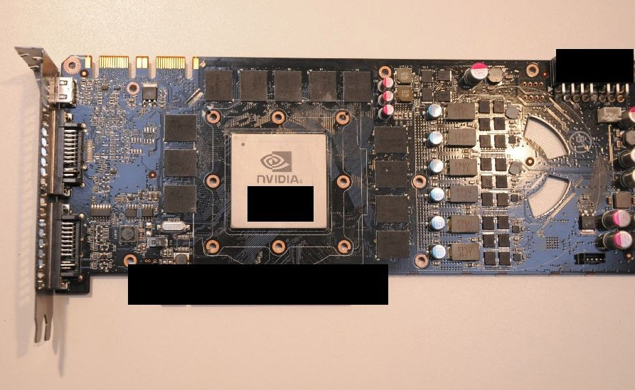
A couple of days after pictures of the PCB and cooling assembly of the GeForce GTX 480 made it to the internet, fresh pictures emerged, this time of the GeForce GTX 470, the slightly toned-down part in the GeForce 400 series. The GTX 470, like the GTX 480, is based on NVIDIA's GF100 core. The reference design PCB is certainly shorter than that of the GTX 480, and compacts its resources. Since the GTX 470 has a 320-bit wide memory interface, it makes do with 10 memory chips, seen surrounding the GPU from three sides. A simpler VRM is used: 4-phase vGPU and 1-phase vMem. Power is drawn in from two 6-pin power connectors.

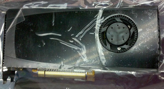
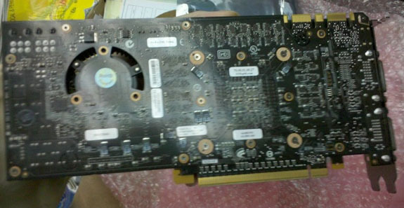
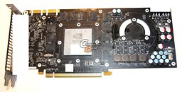
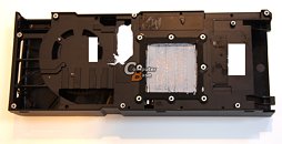
The fan connects over its usual 4-pin PWM-controlled line. Some smart compacting of components made space for two intakes to be cut out, which help the blower draw in some fresh air. The cooling assembly, again is compacted accordingly. Since these new pictures are more clear, we can see that the area over the GPU isn't devoid of a copper surface as earlier thought. In fact, as some community members observed, it is a base with copper heatpipes making direct contact with the GPU. The cooler has protrusions at the right spots to make contact with memory chips and MOSFETs. The GTX 470 is slated to be the more affordable of the GTX 400 series, which will be unveiled on March 26. Follow the source link for equally good quality photography of the GTX 480's PCB.

GeForce GTX 480 PCB and Cooling Assembly Pictured

Sources wanting anonymity sent these pictures of PCB and cooling assembly to sections of the media. The PCB is that of the GeForce GTX 480, and is NVIDIA's reference design. It gives away a fair amount of information about the card that has created quite some hype over the months, which is slated for release on March 26. To begin with, the GF100 GPU on which GTX 480 is based, uses essentially the same type of package as the GT200 and G80. To help cool the large die (with a 3 billion-strong transistor count), an integrated heatspreader (IHS) is used. However, unlike with the G80 and GT200 (past two generations of extreme performance GPUs from NVIDIA), the display logic is integrated into the GPU package, instead of being spun off into NVIO processors.

With 12 memory chips on board, the GPU connects to them over a 384-bit wide memory interface. The reference design board is expected to have 1536 MB (1.5 GB) of memory on it. There's also an unusual amount of simplicity to the board design and choice of components. The GPU is powered by a 6-phase vGPU circuit using more standard DPAK MOSFETs. There is a 2-phase vMem circuit. With wide open spaces in the PCB, NVIDIA actually made two cutouts to help the blower's air intake.

GeForce GTX 470 Graphics Card Pictured

A picture of what NVIDIA's reference design for its next-gen performance graphics card, the GeForce GTX 470, could look like made it to sections of the media. The card is characteristically shorter than the GTX 480 reference design card spotted earlier. The GeForce GTX 470 will be the slightly more affordable part in the series. It is based on NVIDIA's new GF100 graphics core. The GTX 470 has 448 CUDA cores (shader cores), and has a 320-bit wide GDDR5 memory interface. Board partners will sell these cards with 1280 MB of memory. The back of the card shows tracks for 10 memory chips (confirming the 320-bit wide memory interface), and interestingly, also lacks traces for an external display IO processor (like the NVIO2 processor on GT200 based accelerators), cutting down the overall cost of manufacturing. The card draws power from two 6-pin power connectors, and has two SLI fingers for 3-way SLI support. Its connectivity includes two DVI-D, and HDMI.

GeForce GTX 480 Gets Listed

An online PC hardware store, SabrePC.com, has listed a graphics card based on NVIDIA's upcoming DirectX 11 compliant GeForce GTX 480 GPU. And the price: $699 before a $20 rebate. The listing is of a graphics card by NVIDIA partner XFX.

The specifications known at this point in time are that the GeForce GTX 480 is based on NVIDIA's GF100 graphics processor. It is DirectX 11 compliant, and has 512 shader units (dubbed CUDA cores), a 384-bit wide GDDR5 memory interface, and multiple tessellation units. NVIDIA is expected to announce the card along with a cheaper variant, the GeForce GTX 470, later this quarter. By early Q2, the company expects healthy inventories.

NVIDIA GF100 Graphics Card Chugs Along at CES

NVIDIA's next generation graphics card based on the Fermi architecture, whose consumer variant is internally referred to as GF100 got to business at the CES event being held in Las Vegas, USA, performing live demonstration of its capabilities. The demo PC is housing one such accelerator which resembles the card in past sightings. Therefore it is safe to assume this is what the reference NVIDIA design of GF100 would look like. The accelerator draws power from 6-pin and 8-pin power connectors. It has no noticeable back-plate, a black PCB, and a cooler shroud with typical NVIDIA styling. The demo rig was seen running Unigine Heaven in a loop showing off the card's advanced tessellation capabilities in DirectX 11 mode. The most recent report suggests that its market availability can be expected in March, later this year. No performance figures have been made public as yet.
A short video clip after the break.
Return to Keyword Browsing
Apr 24th, 2024 20:38 EDT change timezone

New Forum Posts

Popular Reviews

Controversial News Posts