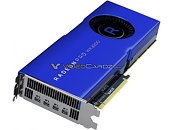
News Posts matching #HBM2

Return to Keyword Browsing

SK hynix Inc. Reports Third Quarter 2019 Results

SK hynix Inc. today announced financial results for its third quarter 2019 ended on September 30, 2019. The consolidated third quarter revenue was 6.84 trillion won while the operating profit amounted to 473 billion won and the net income 495 billion won. Operating margin and net margin for the quarter was 7%.

The revenue in the third quarter increased by 6% quarter-over-quarter (QoQ) as demand began to pick up. However, the operating profit fell by 26% QoQ as DRAM unit cost reduction was not enough to offset the price drop. DRAM bit shipments increased by 23% QoQ as the Company actively responded to the new products in the mobile market and purchases from some data center customers also increased. DRAM prices remained weak during the quarter, leading to a 16% drop in the average selling price, with the decline smaller than the previous quarter.

Samsung Develops Industry's First 12-Layer 3D-TSV Chip Packaging Technology

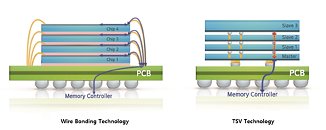
Samsung Electronics Co., Ltd., a world leader in advanced semiconductor technology, today announced that it has developed the industry's first 12-layer 3D-TSV (Through Silicon Via) technology. Samsung's new innovation is considered one of the most challenging packaging technologies for mass production of high-performance chips, as it requires pinpoint accuracy to vertically interconnect 12 DRAM chips through a three-dimensional configuration of more than 60,000 TSV holes, each of which is one-twentieth the thickness of a single strand of human hair.

The thickness of the package (720 µm) remains the same as current 8-layer High Bandwidth Memory-2 (HBM2) products, which is a substantial advancement in component design. This will help customers release next-generation, high-capacity products with higher performance capacity without having to change their system configuration designs. In addition, the 3D packaging technology also features a shorter data transmission time between chips than the currently existing wire bonding technology, resulting in significantly faster speed and lower power consumption.

AMD "Navi 14" and "Navi 12" GPUs Detailed Some More

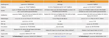
The third known implementation of AMD's "Navi" generation of GPUs with RDNA architecture is codenamed "Navi 14." This 7 nm chip is expected to be a cut-down, mainstream chip designed to compete with a spectrum of NVIDIA GeForce GTX 16-series SKUs, according to a 3DCenter.org report. The same report sheds more light on the larger "Navi 12" GPU that could power faster SKUs competing with the likes of the GeForce RTX 2080 and RTX 2080 Super. The two follow the July launch of the architecture debut with "Navi 10." There doesn't appear to be any guiding logic behind the numerical portion of the GPU codename. When launched, the pecking order of the three Navi GPUs will be "Navi 12," followed by "Navi 10," and "Navi 14."

"Navi 14" is expected to be the smallest of the three, with an estimated 170 mm² die-area, about 24 RDNA compute units (1,536 stream processors), and expected to feature a 128-bit wide GDDR6 memory interface. It will be interesting to see how AMD carves out an SKU that can compete with the GTX 1660 Ti, which has 6 GB of 192-bit GDDR6 memory. The company would have to wait for 16 Gbit (2 GB) GDDR6 memory chips, or piggy-back eight 8 Gbit chips to achieve 8 GB, or risk falling short of recommended system requirements of several games at 1080p, if it packs just 4 GB of memory.

Intel Ships Stratix 10 DX FPGAs, VMWare Among Early Partners

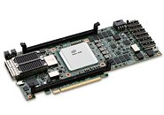
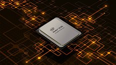
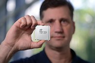
Intel today announced shipments of new Intel Stratix 10 DX field programmable gate arrays (FPGA). The new FPGAs are designed to support Intel Ultra Path Interconnect (Intel UPI), PCI-Express (PCIe) Gen4 x16 and a new controller for Intel Optane technology to provide flexible, high-performance acceleration. VMware is one of many early access program participants.

"Intel Stratix 10 DX FPGAs are the first FPGAs designed to combine key features that dramatically boost acceleration of workloads in the cloud and enterprise when used with Intel's portfolio of data center solutions. No other FPGA currently offers this combination of features for server designs based on future select Intel Xeon Scalable processors," said David Moore, Intel vice president and general manager, FPGA and Power Products, Network and Custom Logic Group.

Control Can Use Up to 18.5GB of Video Memory

"Control" by Remedy is the season's hottest AAA release, not just because it's an above-average story-driven action RPG, but also because it's an eye candy-shop. With the ability to use NVIDIA RTX real-time raytracing across a multitude of features, the game is particularly heavy on graphics hardware. Tweaktown tested the game's stability at extremely high display resolutions, including 8K, and found that the game can use up to 18.5 GB of video memory, when running in DirectX 12 with RTX enabled. There's only one client-segment graphics card capable of that much memory, the $2,499 NVIDIA TITAN RTX, which ships with 24 GB of GDDR6 memory. Its nearest client-segment neighbor is the AMD Radeon VII, but it only packs 16 GB of HBM2.

When a game needs more video memory than your graphics card has, Windows has an elaborate memory management system that sheds some of that memory onto your system's main memory, and the swap file progressively (at reduced performance, of course). Video memory usage drops like a rock between 8K and 4K UHD (which is 1/4th the pixels as 8K). With all RTX features enabled and other settings maxed out, "Control" only uses 8.1 GB of video memory. What this also means is that video cards with just 8 GB of memory are beginning fall short of what it takes to game at 4K. The $699 GeForce RTX 2080 Super only has 8 GB. The RTX 2080 Ti, with its 11 GB of memory has plenty of headroom and muscle. Find other interesting observations in the source link below.

AMD Retires the Radeon VII Less Than Five Months Into Launch

AMD has reportedly discontinued production of its flagship Radeon VII graphics card. According to a Cowcotland report, AMD no longer finds it viable to produce and sell the Radeon VII at prices competitive to NVIDIA's RTX 2080, especially when its latest Radeon RX 5700 XT performs within 5-12 percent of the Radeon VII at less than half its price. AMD probably expects custom-design RX 5700 XT cards to narrow the gap even more. The RX 5700 XT has a much lesser BOM (bill of materials) cost compared to the Radeon VII, due to the simplicity of its ASIC, a conventional GDDR6 memory setup, and far lighter electrical requirements.

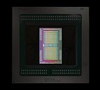
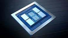
In stark contrast to the RX 5700 XT, the Radeon VII is based on a complex MCM (multi-chip module) that has not just a 7 nm GPU die, but also four 32 Gbit HBM2 stacks, and a silicon interposer. It also has much steeper VRM requirements. Making matters worse is the now-obsolete "Vega" architecture it's based on, which loses big time against "Navi" at performance/Watt. The future of AMD's high-end VGA lineup is uncertain. Looking at the way "Navi" comes close to performance/Watt parity with NVIDIA on the RX 5700, AMD may be tempted to design a larger GPU die based on "Navi," with a conventional GDDR6-based memory sub-system, to take another swing at NVIDIA's high-end.

AMD Announces the Radeon Pro Vega II and Pro Vega II Duo Graphics Cards

AMD today announced the Radeon Pro Vega II and Pro Vega II Duo graphics cards, making their debut with the new Apple Mac Pro workstation. Based on an enhanced 32 GB variant of the 7 nm "Vega 20" MCM, the Radeon Pro Vega II maxes out its GPU silicon, with 4,096 stream processors, 1.70 GHz peak engine clock, 32 GB of 4096-bit HBM2 memory, and 1 TB/s of memory bandwidth. The card features both PCI-Express 3.0 x16 and InfinityFabric interfaces. As its name suggests, the Pro Vega II is designed for professional workloads, and comes with certifications for nearly all professional content creation applications.

The Radeon Pro Vega II Duo is the first dual-GPU graphics card from AMD in ages. Purpose built for the Mac Pro (and available on the Apple workstation only), this card puts two fully unlocked "Vega 20" MCMs with 32 GB HBM2 memory each on a single PCB. The card uses a bridge chip to connect the two GPUs to the system bus, but in addition, has an 84.5 GB/s InfinityFabric link running between the two GPUs, for rapid memory access, GPU and memory virtualization, and interoperability between the two GPUs, bypassing the host system bus. In addition to certifications for every conceivable content creation suite for the MacOS platform, AMD dropped in heavy optimization for the Metal 3D graphics API. For now the two graphics cards are only available as options for the Apple Mac Pro. The single-GPU Pro Vega II may see standalone product availability later this year, but the Pro Vega II Duo will remain a Mac Pro-exclusive.

AMD Memory Tweak Tool Lets You OC and Tweak AMD Radeon Memory Timings On-the-fly

Eliovp, who describes himself on GitHub as a Belgian [crypto] mining enthusiast, created what could go down as the best thing that happened to AMD Radeon users all decade. The AMD Memory Tweak Tool is a Windows and Linux based GUI utility that lets you not just overclock AMD Radeon graphics card memory on the fly, but also lets you tweak its memory timings. Most timings apply live, while your machine is running within Windows/Linux GUI, some require memory retraining via a reboot, which means they can't be changed at this time, because rebooting reverts the timings to default. The author is trying to figure out a way to run memory training at runtime, which would let you change those timings, too, in the future. While you're at it, the tool also lets you play with GPU core frequency and fan-control.

The AMD Memory Tweak tool supports both Windows and Linux (GUI), and works with all recent AMD Radeon GPUs with GDDR5 and HBM2 memory types. It requires Radeon Software Adrenalin 19.4.1 or later in case of Windows, or amdgpu-pro ROCM to be actively handling the GPU in case of Linux. The Linux version further has some dependencies, such as pciutils-dev, libpci-dev, build-essential, and git. The source-code for the utility is up on GitHub for you to inspect and test.

DOWNLOAD: AMD Memory Tweak Tool by Eliovp

EK Water Blocks Releases EK-Vector Series Water Blocks for AMD Radeon VII

EK Water Blocks, the leading premium computer liquid cooling gear manufacturer, is releasing EK-Vector Radeon VII water blocks that are compatible with reference design AMD Radeon VII graphics cards. This kind of efficient cooling will allow your high-end graphics card to reach higher boost clocks, thus providing more overclocking headroom and more performance during gaming or other GPU intense tasks.

This water block directly cools the GPU, 16GB of HBM2 memory, and VRM (voltage regulation module) as cooling liquid is channeled directly over these critical areas. These newly developed water blocks feature a redesigned cooling engine that has a larger footprint compared to the previous generation of EK Full Cover water blocks. This results in a larger surface area for heat transfer which increases the thermal performance of these water blocks.

Samsung Electronics Introduces New Flashbolt HBM2E High Bandwidth Memory

Samsung Electronics Co., Ltd., the world leader in advanced semiconductor technology, today announced its new High Bandwidth Memory (HBM2E) product at NVIDIA's GPU Technology Conference (GTC) to deliver the highest DRAM performance levels for use in next-generation supercomputers, graphics systems, and artificial intelligence (AI).

The new solution, Flashbolt , is the industry's first HBM2E to deliver a 3.2 gigabits-per-second (Gbps) data transfer speed per pin, which is 33 percent faster than the previous-generation HBM2. Flashbolt has a density of 16Gb per die, double the capacity of the previous generation. With these improvements, a single Samsung HBM2E package will offer a 410 gigabytes-per-second (GBps) data bandwidth and 16 GB of memory.

GIGABYTE Announces its Radeon VII Graphics Card

GIGABYTE, the world's leading premium gaming hardware manufacturer, today announced the launch of Radeon VII HBM2 16G, the latest Radeon VII graphics cards built upon the world's first 7nm gaming GPU. Based on the enhanced second-generation AMD 'Vega' architecture, Radeon VII is equipped with 3840 stream processors and 16GB of ultra-fast HBM2 memory (second-generation High-Bandwidth Memory). It is designed to deliver exceptional performance and amazing experiences for the latest AAA, e-sports and Virtual Reality (VR) titles, demanding 3D rendering and video editing applications, and next-generation compute workloads.

According to the AMD official website, the Radeon VII graphics card enables high-performance gaming and ultra-high quality visuals. Ground-breaking 1 TB/s memory bandwidth and a 4,096-bit memory interface paves the way for ultra-high resolution textures, hyper-realistic settings and life-like characters. With the high speeds of today's graphics cards, framerates often exceed the monitor refresh rate, causing stuttering and tearing.

PowerColor Also Unveils its Reference Radeon VII

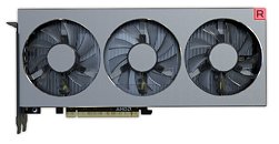
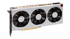
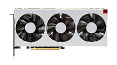
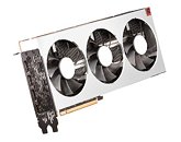
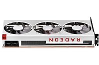
Amidst breaking news about PowerColor designing what could be the first custom-design Radeon VII graphics card, the company also unveiled its reference-design Radeon VII card, the AXVII 16GBHBM2-3DH. This card sticks to AMD's reference design clock speeds of up to 1750 MHz boost, and up to 1800 MHz "peak" clock speeds, with the memory ticking at 1000 MHz. It implements the slick, solid-aluminium triple-fan stock cooling solution AMD designed for this card. Drawing power from a pair of 8-pin PCIe power connectors, the card puts out three DisplayPort 1.4 and an HDMI 2.0b. Based on the 7 nm "Vega 20" silicon, the Radeon VII packs 3,840 stream processors, 240 TMUs, 64 ROPs, and a 4096-bit wide HBM2 memory interface, holding 16 GB of memory. It's likely that PowerColor will sell this card close to AMD's MSRP for this card, USD $699.

Sapphire Launches its Radeon VII, AMD Reserving 1.80 GHz Boost for Direct Sales?

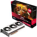
Sapphire is among the first AMD add-in-board (AIB) partners to launch a Radeon VII graphics card. The card sticks to AMD reference board design, which the company unveiled at its CES 2019 keynote. Interestingly, its GPU engine boost frequency is set at 1750 MHz, which is less than the 1800 MHz boost frequency figure that was mentioned by the company earlier. Could it be that AMD is reserving 1800 MHz for cards directly sold on AMD.com? The memory frequency is unchanged at 1000 MHz, which works out to an HBM2 memory bandwidth of 1 TB/s. Sapphire's box for this card lists out key specifications upfront, and also features the Vega II logo. It's likely that the card will be sold at the baseline price of $699, given that there are no other variants of this card, not even custom-design.

AMD Radeon VII Detailed Some More: Die-size, Secret-sauce, Ray-tracing, and More

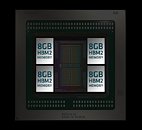
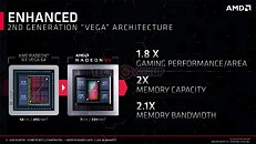
AMD pulled off a surprise at its CES 2019 keynote address, with the announcement of the Radeon VII client-segment graphics card targeted at gamers. We went hands-on with the card earlier this week. The company revealed a few more technical details of the card in its press-deck for the card. To begin with, the company talks about the immediate dividends of switching from 14 nm to 7 nm, with a reduction in die-size from 495 mm² on the "Vega 10" silicon to 331 mm² on the new "Vega 20" silicon. The company has reworked the die to feature a 4096-bit wide HBM2 memory interface, the "Vega 20" MCM now features four 32 Gbit HBM2 memory stacks, which make up the card's 16 GB of memory. The memory clock has been dialed up to 1000 MHz from 945 MHz on the RX Vega 64, which when coupled with the doubled bus-width, works out to a phenomenal 1 TB/s memory bandwidth.

We know from AMD's late-2018 announcement of the Radeon Instinct MI60 machine-learning accelerator based on the same silicon that "Vega 20" features a total of 64 NGCUs (next-generation compute units). To carve out the Radeon VII, AMD disabled 4 of these, resulting in an NGCU count of 60, which is halfway between the RX Vega 56 and RX Vega 64, resulting in a stream-processor count of 3,840. The reduced NGCU count could help AMD harvest the TSMC-built 7 nm GPU die better. AMD is attempting to make up the vast 44 percent performance gap between the RX Vega 64 and the GeForce RTX 2080 with a combination of factors.
AMD Radeon VII Hands On at CES 2019

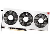
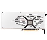
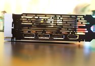
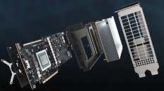
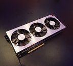
While many have watched or at the very least seen our coverage of AMD's live stream at CES 2019, it just can't compare to seeing the latest graphics card from the company up close and personal. Therefore as soon as we had the opportunity, we took a closer look at the AMD Radeon VII and let us just say the reference card is indeed a bit fancy. The shroud itself is made of metal and has a very similar look and feel to the one used on the Radeon RX Vega 64 liquid cooled reference cards. However, instead of using an AIO for this release AMD instead opted for three uniform fans and a massive heatsink. Not only does this make the card more compatible with small form factor systems, it is also less of a hassle to install. Display outputs consist of 3x DisplayPort and 1x HDMI. Sadly AMD did not include a VirtualLink port (USB Type-C) like NVIDIA for VR headsets, which is rather odd considering AMD is also part of the VirtualLink consortium.

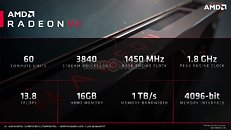
Power delivery is handled by two 8-pin PCIe power connectors giving the card access to a theoretical limit of 375-watts which is 75-watts more than its 300-watt TDP. Considering the Radeon VII has the same power level as the Vega 64 it offers 25% more performance at the same power level. Compute unit count falls between the Vega 56 and Vega 64 at precisely 60 CUs. That said, a few missing CUs are of no consequence when you consider how close the Vega 56 performed to the Vega 64 once tweaked. As for clock speeds AMD has stated the Radeon VII will have a 1.8 GHz core clock, while the 16 GB of HBM2 will deliver 1 TB/s of memory bandwidth over the 4096-bit memory interface.

AMD Announces the Radeon VII Graphics Card: Beats GeForce RTX 2080

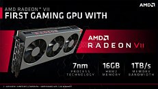
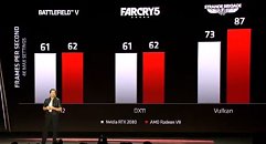
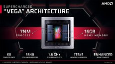
AMD today announced the Radeon VII (Radeon Seven) graphics card, implementing the world's first GPU built on the 7 nm silicon fabrication process. Based on the 7 nm "Vega 20" silicon with 60 compute units (3,840 stream processors), and a 4096-bit HBM2 memory interface, the chip leverages 7 nm to dial up engine clock speeds to unprecedented levels (above 1.80 GHz possibly). CEO Lisa Su states that the Radeon VII performs competitively with NVIDIA's GeForce RTX 2080 graphics card. The card features a gamer-friendly triple-fan cooling solution with a design focus on low noise. AMD is using 16 GB of 4096-bit HBM2 memory. Available from February 7th, the Radeon VII will be priced at USD $699.

Update: We went hands on with the Radeon VII card at CES.

AMD's CES 2019 Keynote - Stream & Live Blog

CPUs or GPUs? Ryzen 3000 series up to 16 cores or keeping their eight? Support for raytracing? Navi or die-shrunk Vega for consumer graphics? The questions around AMD's plans for 2019 are still very much in the open, but AMD's Lisa Su's impending livestream should field the answers to many of these questions, so be sure to watch the full livestream, happening in just a moment.

You can find the live stream here, at YouTube.

18:33 UTC: Looking forward, Lisa mentioned a few technology names without giving additional details: "... when you're talking about future cores, Zen 2, Zen 3, Zen 4, Zen 5, Navi, we're putting all of these architectures together, in new ways".

18:20 UTC: New Ryzen 3rd generation processors have been teased. The upcoming processors are based on Zen 2, using 7 nanometer technology. AMD showed a live demo of Forza Horizon 4, using Ryzen third generation, paired with Radeon Vega VII, which is running "consistently over 100 FPS at highest details at 1080p resolution". A second demo, using Cinebench, pitted an 8-core/16-thread Ryzen 3rd generation processor against the Intel Core i9-9900K. The Ryzen CPU was "not final frequency, an early sample". Ryzen achieved a score of 2057 using 135 W, while Intel achieved a score of 2040 using 180 W.. things are looking good for Ryzen 3rd generation indeed. Lisa also confirmed that next-gen Ryzen will support PCI-Express 4.0, which doubles the bandwidth per lane over PCI-Express 3.0. Ryzen third generation will run on the same AM4 infrastructure as current Ryzen; all existing users of Ryzen can simply upgrade to the new processors, when they launch in the middle of 2019 (we think Computex).
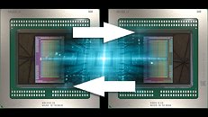
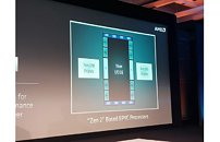
Ryzen third generation uses a chiplet design. The smaller die on the right contains 8-cores/16-threads using 7 nanometer technology. The larger die on the left is the IO die, which consists of things like the memory controller and PCI-Express connectivity, to shuffle data between the CPU core die and the rest of the system.

Vega II Logo Trademarked by AMD

AMD late November filed a trademark application with the USPTO for a new logo, for its second generation "Vega" graphics architecture, built around the 7 nm silicon fabrication process. The logo looks similar to the original Vega "V," with two bands marking out the Roman numeral II (2). This logo could appear on the product and marketing on a series of new Radeon Pro and Radeon Instinct (and possibly even gaming-grade Radeon RX?) graphics cards based on AMD's new "Vega 20" multi-chip module. This chip features a doubling in memory bandwidth thanks to its 4096-bit wide HBM2 interface, and the optical shrink of the GPU die to the 7 nm node could enable AMD to dial up engine clocks significantly.

It Can't Run Crysis: Radeon Instinct MI60 Only Supports Linux

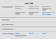
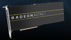
AMD recently announced the Radeon Instinct MI60, a GPU-based data-center compute processor with hardware virtualization features. It takes the crown for "the world's first 7 nm GPU." The company also put out specifications of the "Vega 20" GPU it's based on: 4,096 stream processors, 4096-bit HBM2 memory interface, 1800 MHz engine clock-speed, 1 TB/s memory bandwidth, 7.4 TFLOP/s peak double-precision (FP64) performance, and the works. Here's the kicker: the company isn't launching this accelerator with Windows support. At launch, AMD is only releasing x86-64 Linux drivers, with API support for OpenGL 4.6, Vulkan 1.0, and OpenCL 2.0, along with AMD's ROCm open ecosystem. The lack of display connector already disqualifies this card for most workstation applications, but with the lack of Windows support, it is also the most expensive graphics card that "can't run Crysis." AMD could release Radeon Pro branded graphics cards based on "Vega 20," which will ship with Windows and MacOS drivers.

AMD Unveils World's First 7 nm GPUs - Radeon Instinct MI60, Instinct MI50

AMD today announced the AMD Radeon Instinct MI60 and MI50 accelerators, the world's first 7nm datacenter GPUs, designed to deliver the compute performance required for next-generation deep learning, HPC, cloud computing and rendering applications. Researchers, scientists and developers will use AMD Radeon Instinct accelerators to solve tough and interesting challenges, including large-scale simulations, climate change, computational biology, disease prevention and more.

"Legacy GPU architectures limit IT managers from effectively addressing the constantly evolving demands of processing and analyzing huge datasets for modern cloud datacenter workloads," said David Wang, senior vice president of engineering, Radeon Technologies Group at AMD. "Combining world-class performance and a flexible architecture with a robust software platform and the industry's leading-edge ROCm open software ecosystem, the new AMD Radeon Instinct accelerators provide the critical components needed to solve the most difficult cloud computing challenges today and into the future."

AMD Unveils "Zen 2" CPU Architecture and 7 nm Vega Radeon Instinct MI60 at New Horizon

AMD today held its "New Horizon" event for investors, offering guidance and "color" on what the company's near-future could look like. At the event, the company formally launched its Radeon Instinct MI60 GPU-based compute accelerator; and disclosed a few interesting tidbits on its next-generation "Zen 2" mircroarchitecture. The Instinct MI60 is the world's first GPU built on the 7 nanometer silicon fabrication process, and among the first commercially available products built on 7 nm. "Rome" is on track to becoming the first 7 nm processor, and is based on the Zen 2 architecture.

The Radeon Instinct MI60 is based on a 7 nm rendition of the "Vega" architecture. It is not an optical shrink of "Vega 10," and could have more number-crunching machinery, and an HBM2 memory interface that's twice as wide that can hold double the memory. It also features on-die logic that gives it hardware virtualization, which could be a boon for cloud-computing providers.

Blackmagic Design Announces Blackmagic eGPU Pro

Blackmagic Design today announced the Blackmagic eGPU Pro, an external graphics processor featuring the blazingly fast AMD Radeon RX Vega 56 graphics processor. Designed to accelerate pro creative software such as DaVinci Resolve, 3D games and VR, the Blackmagic eGPU Pro delivers nearly twice the performance of the original Blackmagic eGPU model and up to 22x faster performance than the built-in graphics on a 13-inch MacBook Pro.

The Blackmagic eGPU Pro features a built-in AMD Radeon RX Vega 56, two Thunderbolt 3 ports, a new DisplayPort for connecting 5K displays, HDMI 2.0, 85W of charging power and four USB 3.1 connections. Designed in collaboration with Apple, the integrated design brings cutting-edge workstation-class graphics processing and computational acceleration to customers working in professional video, playing 3D games or using the latest virtual reality software.

AMD "Vega 20" GPU Not Before Late Q1-2019

AMD "Vega 20" is a new GPU based on existing "Vega" graphics architecture, which will be fabbed on the 7 nanometer silicon fabrication process, and bolstered with up to 32 GB of HBM2 memory across a 4096-bit memory interface that's double the bus-width of "Vega 10". AMD CEO Lisa Su already exhibited a mock-up of this chip at Computex 2018, with an word that alongside its "Zen 2" based EPYC enterprise processors, "Vega 20" will be the first 7 nm GPU. AMD could still make good on that word, only don't expect to find one under your tree this Holiday.

According to GamersNexus, the first "Vega 20" products won't launch before the turn of the year, and even in 2019, one can expect product launches till the end of Q1 (before April). GamersNexus cites reliable sources hinting at the later-than-expected arrival of "Vega 20" as part of refuting alleged "Final Fantasy XV" benchmarks of purported "Vega 20" engineering samples doing rounds on the web. Lisa Su stressed the importance of data-center GPUs in AMD's Q3-2018 earnings call, which could hint at the possibility of AMD allocating its first "Vega 20" yields to high-margin enterprise brands such as Radeon Pro and Radeon Instinct.

AMD 7nm "Vega" by December, Not a Die-shrink of "Vega 10"

AMD is reportedly prioritizing its first 7 nanometer silicon fabrication allocations to two chips - "Rome," and "Vega 20." Rome, as you'll recall, is the first CPU die based on the company's "Zen 2" architecture, which will build the company's 2nd generation EPYC enterprise processors. "Vega 20," on the other hand, could be the world's first 7 nm GPU.

"Vega 20" is not a mere die-shrink of the "Vega 10" GPU die to the 7 nm node. For starters, it is flanked by four HBM2 memory stacks, confirming it will feature a wider memory interface, and support for up to 32 GB of memory. AMD at its Computex event confirmed that "Vega 20" will build Radeon Instinct and Radeon Pro graphics cards, and that it has no plans to bring it to the client-segment. That distinction will be reserved for "Navi," which could only debut in 2019, if not later.
AMD Radeon Pro WX 8200 Detailed

AMD is giving final touches to the new Radeon Pro WX 8200 professional graphics card. Launched over a year following the Radeon Pro WX 9100, the WX 8200 has a leaner feature-set, while continuing to be based on AMD's current IP. The card still uses the 14 nm "Vega 10" MCM, but with a core-config akin to that of the RX Vega 56. You get 56 NGCUs working out to 3,584 stream processors, 224 TMUs, 64 ROPs, and a 4096-bit wide HBM2 memory interface, handling 16 GB of memory on this card. The air-cooled card also has a leaner connectivity load-out, with just four mini-DisplayPort 1.4 connectors (the WX 9100 comes with six). Its 8-pin + 6-pin connectors are positioned at the rear-end to be SSI workstation-friendly. The card surfaced on CompuBench database, in which its performance numbers are only slightly behind those of the WX 9100, but significantly better than the "Polaris 20" based WX 7100. AMD is expected to launch this card at SIGGRAPH 2018.
Return to Keyword Browsing
Apr 16th, 2024 01:43 EDT change timezone

New Forum Posts

Popular Reviews

Controversial News Posts