News Posts matching #Intel

Return to Keyword Browsing

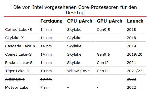
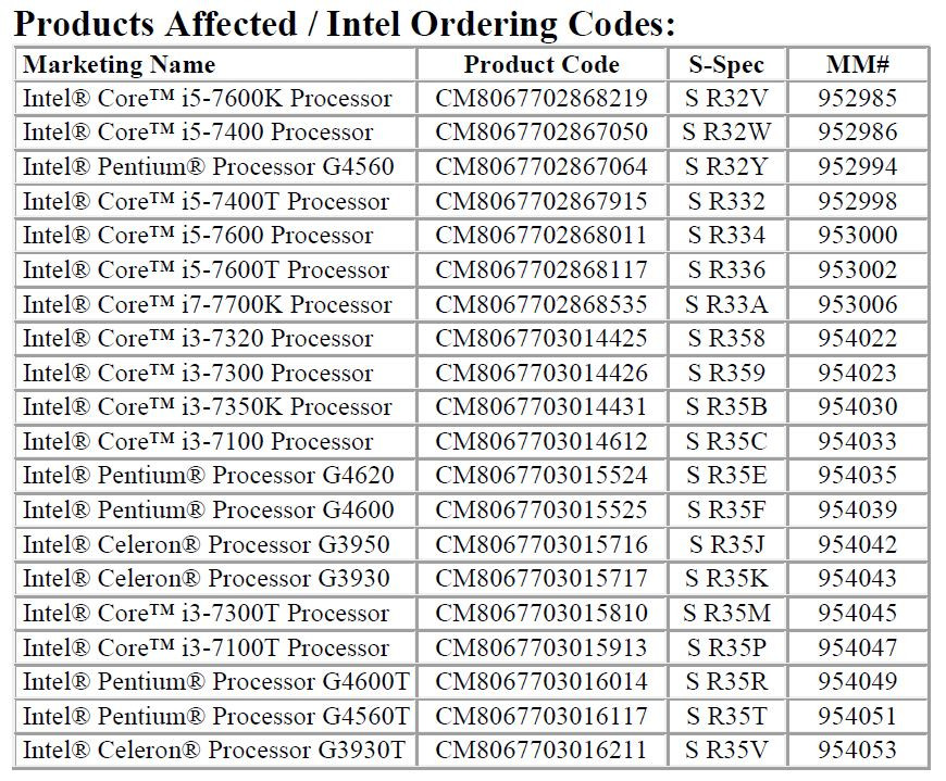
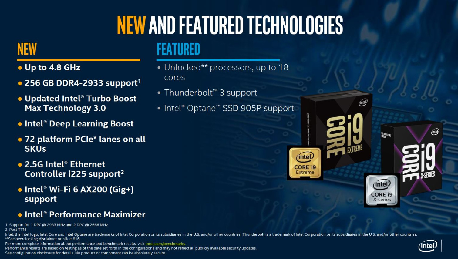
Intel Scraps 10nm for Desktop, Brazen it Out with 14nm Skylake Till 2022?

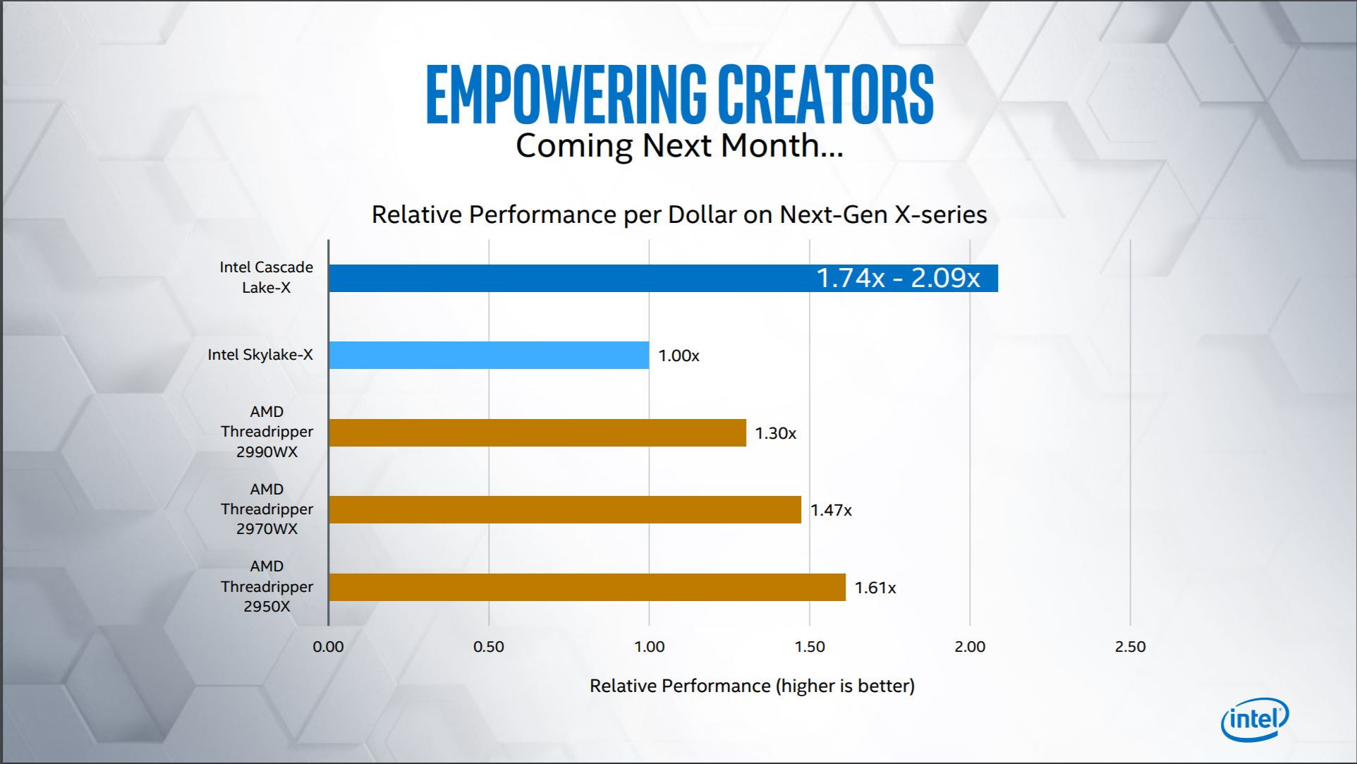
In a shocking piece of news, Intel has reportedly scrapped plans to launch its 10 nm "Ice Lake" microarchitecture on the client desktop platform. The company will confine its 10 nm microarchitectures, "Ice Lake" and "Tiger Lake" to only the mobile platform, while the desktop platform will see derivatives of "Skylake" hold Intel's fort under the year 2022! Intel gambles that with HyperThreading enabled across the board and increased clock-speeds, it can restore competitiveness with AMD's 7 nm "Zen 2" Ryzen processors with its "Comet Lake" silicon that offers core-counts of up to 10.

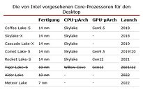
"Comet Lake" will be succeeded in 2021 by the 14 nm "Rocket Lake" silicon, which somehow combines a Gen12 iGPU with "Skylake" derived CPU cores, and possibly increased core-counts and clock speeds over "Comet Lake." It's only 2022 that Intel will ship out a truly new microarchitecture on the desktop platform, with "Meteor Lake." This chip will be built on Intel's swanky 7 nm EUV silicon fabrication node, and possibly integrate CPU cores more advanced than even "Willow Cove," possibly "Golden Cove."

Intel's Gargantuan Next-gen Enterprise CPU Socket is LGA4677

Intel has finalized design of its next-generation Xeon Scalable enterprise CPU socket for its "Sapphire Rapids" processors. Called LGA4677, the socket succeeds LGA3647, and is bound for a 2021 market release. Intel will have transitioned to its advanced 7 nm EUV silicon fabrication node on the CPU front, and has adopted an "enterprise-first" strategy for the node. LGA4677 will be designed to handle the extremely high bandwidth of PCI-Express Gen 5, which doubles bandwidth over PCIe gen 4.0, and adds several enterprise-specific features Intel is rolling out in advance as part of its CXL interconnect. These details, along with a prototype LGA4189 socket, was revealed at an exhibit by TE Connectivity, a company that manufactures the socket. The additional pin-count could enable Intel to not just deploy PCI-Express Gen 5, but also expand I/O in other directions, such as more memory channels, dedicated Persistent Memory I/O, etc.

Intel Core i3-10100 Put Through SANDRA, Beats i3-9100 by 31% in Multimedia Tests

Intel's 10th generation Core desktop processor lineup, based on the 14 nm "Comet Lake" silicon, will begin with the Core i3-10100 succeeding the Core i3-9100 and i3-8100. To squeeze the most out of the microarchitecture that's essentially identical to "Skylake," Intel has decided to enable HyperThreading across the Core processor family, which means the i3-10100 is a 4-core/8-thread chip. Interestingly, Intel has given it just 6 MB of shared L3 cache. It's likely that the slightly beefed up i3-103xx will be differentiated with 8 MB of L3 cache. The chip has the same 3.60 GHz nominal frequency, and an unknown degree of Turbo Boost. The current-gen i3-9100 features Turbo Boost, so it's likely that its successor will also get the feature.

A SiSoft SANDRA online database entry for the i3-10100 surfaced, where it has an overall score of 382.61 MPix/s using multimedia tests, a significal step up from the roughly 290 MPix/s of the i3-9100 (a 31 percent performance increase). This increase in performance can be attributed to HyperThreading, as SANDRA's multimedia tests leverage it efficiently. Intel is expected to launch the Core i3-10100 around the $120 mark, competing with AMD's Ryzen 3 3200G.

Next-Gen Intel Core i3 to Sport Hyper Threading?

TUM_APISAK has done of his well-regarded snoopings again, and this one could have relevant information for the democratization of threads in next-gen Intel products. Intel has been slowly (as they can) increasing the amount of cores and threads in their respective product lines across i3, i5, and i7 CPUs after AMD's Ryzen onslaught. Luckily, from two core, four-thread Core i3 of a few years ago, we now seem to be entering a new era for entry-level computing, with a new SiSoftware benchmark seemingly showing an Intel next-gen "Comet Lake" Core i3 CPU sporting 4 physical threads with Hyper Threading enabled (so, basically, the equivalent of Skylake Core i7's from just three years ago).

The benchmark submission lists what appears to be a four-core, eight-thread Core i3-10100. It sports a 3.6 GHz base clock, which likely isn't final, so take that frequency with a grain of salt. This shuffle in the low-end definitely means an upscale in Intel's more powerful lineups, with HyperThreading likely being active for all of their product stack across Comet Lake - 4C, 8T Core i3; 6C, 12T Core i5; 8C, 16T Core i7; and a likely 10C, 20T Core i9 10900K that straddles the line between consumer and HEDT platforms. Of course, remember these are still built upon the 14 nm process, give or take a few "+" symbols, so don't expect too much in terms of energy efficiency gains.

Intel Discontinues Almost the Entire 7th Generation Core Desktop Processor Series

Intel late Thursday, through a product change notification, announced the discontinuation of almost its entire 7th generation Core "Kaby Lake" desktop processor series. This includes most chips across the Core i3, Core i5, Core i7, Pentium, and Celeron desktop chips based on the 14 nm+ "Kaby Lake-S" silicon, across both retail boxed and tray packages. These chips formed Intel's main product lineup through 2017, and had to be quickly succeeded by the 8th generation "Coffee Lake" with the advent of AMD Ryzen. To clear out its inventory, Intel will accept discontinuance orders for these chips until April 2020. A discontinuance order can only be placed by a customer who has previously ordered these exact chips. The last of these orders will be shipped out by October 2020.

Intel Discontinues Omni-Path Enabled Xeon Processors

Intel's Omni-Path technology has been used primarily in high performance computing market, in order to provide high speed interconnect between Intel Xeon CPUs, with speeds reaching around 100 Gbps. Accompanied by different design and system integration that Omni-Path uses, it was a bit difficult to integrate into server system, while not adding much value that other technologies couldn't match or beat.

Because of these reasons, Intel is now discontinuing its last product capable of utilizing Omni-Path - the first generation Xeon Scalable CPUs. Carrying the suffix "F", these CPUs had an extra connector sticking out of CPU's PCB to enable the Omni-Path functionality (see images bellow). There were eight CPUs manufactured in total that had this extra feature, consisting out of two Xeon Platinum and six Xeon Gold CPUs, which have now reached end of life. Intel states that focus from these CPUs has shifted to other technologies like silicon photonics, which provides much greater speed reaching 100s of gigabits per second. Intel already demonstrated transceivers capable of reaching 400 Gb/s speeds with the magic of light, which will become available in 1H 2020.

Intel Mobility Xe GPUs to Feature Up to Twice the Performance of Previous iGPUs

Intel at the Intel Developer Conference 'IDC' 2019 in Tokyo revealed their performance projections for mobility Xe GPUs, which will supersede their current consumer-bound UHD620 graphics under the Gen 11 architecture. The company is being vocal in that they can achieve an up to 2x performance uplift over their previous generation - but that will likely only take place in specific scenarios, and not as a rule of thumb. Just looking at Intel's own performance comparison graphics goes to show that we're mostly looking at between 50% and 70% performance improvements in popular eSports titles, which are, really, representative of most of the gaming market nowadays.

The objective is to reach above 60 FPS in the most popular eSports titles, something that Gen 11 GPUs didn't manage with their overall IPC and dedicated die-area. We've known for some time that Intel's Xe (as in, exponential) architecture will feature hardware-based raytracing, and the architecture is being developed for scalability that goes all the way from iGPUs to HPC platforms.

Star Wars Jedi: Fallen Order System Requirements Outed

The upcoming single-player Star Wars Jedi: Fallen order will be a tall calling for Respawn. Few franchises are as loved as Star Wars, and this one will definitely leave a mark in the company's legacy. It's unlikely EA will "pull an EA" on the studio even if it flops, though: Apex Legends remains an incredibly successful release form Respawn Entertainment, and it should be enough to hold EA's reins - at least for a while.

The system requirements for the highly-awaited, story-driven single-player game have been outed, and they're in the usual side of things. Minimum requirements call for an AMD FX-6100 or an Intel Core i3-3220, paired with 8 GB of RAM and an AMD Radeon HD 7750 or NVIDIA GeForce GTX 650 - alongside 65 GB of storage. The recommended specs are relatively standard as well, and nothing to throw users in an upgrade fit... We're looking at an AMD AMD Ryzen 7 1700 or an Intel i7-6700K, 16 GB of system RAM, An AMD RX Vega 56 or NVIDIA GTX 1070 graphics cards. Star Wars Jedi: Fallen Order drops on November 15th.

The End of a Collaboration: Intel Announces Discontinuation of Kaby Lake-G with AMD Radeon Vega Graphics

The marriage of Intel and AMD IPs in the form of the Kaby Lake-G processors was met with both surprised grunts from the company and a sense of bewilderment at what could come next. Well, we now know what came next: Intel hiring several high-level AMD employees on the graphics space and putting together its own motley crew of discrete GPU developers, who should be putting out Intel's next-gen high-performance graphics accelerators sometime next year.

The Kaby Lake-G processors, however, showed promise, pairing both Intel's (at the time) IPC dominance and AMD's graphics IP performance and expertise on a single package by placing the two components in the same substrate and connecting them via a PCIe link. A new and succinct Intel notice on the Kaby Lake-G page sets a last order time (January 31, 2020, as the last date for orders, and July 31, 2020, as the date of last shipments), and explains that product market shifts have moved demand from Kaby Lake-G products "to other Intel products". Uptake was always slow on this particular collaboration - most of it, we'd guess, because of the chips' strange footprint arrangement for embedding in systems, which required custom solutions that had to be designed from scratch. And with Intel investing into their own high-performance graphics, it seems clear that there is just no need to flaunt their previous collaborations with other companies in this field. Farewell, Intel-AMD Kaby Lake-G. We barely knew you.

Intel Readies "The Element" - a Next-Generation of Modular PCs

Yesterday Intel hosted an event in London, where it held a presentation and demonstration of new concept product. Simply called "The Element", this new products tries to introduce the concept of modular computing, where you can basically swap out parts and replace them with ease, to users of PCs who wanted this to happen for a long time.

If anyone remembers Razer's project Christine, which unfortunately didn't take off, this product should be of no surprise to them. The Element is a complete PC consisting out of CPU, RAM and Storage, with a PCIe slot attached to it. Featuring plenty of IO options like Thunderbolt, HDMI, Ethernet, USB, and Wi-Fi, The Element is a complete solution for computing. For the demo Intel soldered a BGA Xeon CPU with room for two SODIMM slots for memory and two M.2 ports for storage expansion, all cooled by a blower fan directly cooling the CPU heatsink. Power is supplied from PCIe slot (75 Watts) and 8 pin connector which would come from a regular PSU. There is also an option for the card to be powered by a 19 V power source if external power brick is provided.

Intel Cuts Prices of iGPU-devoid 9th Gen Core F and KF SKUs by up to 20 Percent

Intel Monday revised prices of select 9th generation Core "Coffee Lake Refresh" desktop processor models. These price cuts target the "F" and "KF" brand extensions, which denote a lack of integrated graphics. The price cuts range from 5 percent to 20 percent, and cover key fast-moving SKUs popular with the DIY gaming PC crowd that likes to pair these chips with discrete graphics cards. The entry-level Core i3-9100F gets the biggest cut of the lot. The 4-core/4-thread chip is now selling for USD $97, a 20 percent cut from its $122 MSRP.

Other noteworthy cuts include the popular Core i5-9400F 6-core/6-thread processor, which is now going for $157, compared to its $182 original price. This chip has seen sub-$160 pricing in promotional sales on popular e-tailers such as Newegg. The Core i7-9700F and i7-9700KF are the other popular SKUs among the premium gaming PC build crowd. The two 8-core/8-thread chips are now priced at $298 and $349, respectively. Leading the pack is the Core i9-9900KF, which is going for $463, a small 5% saving over the i9-9900K which you can spend elsewhere, such as slightly faster RAM.

Intel Marketing Tries to Link Stability to Turbo Boost

There is no correlation between CPU frequency boosting behavior and system stability. Intel today launched its "10th generation" Core X HEDT processors, with core-counts ranging between 10 to 18, priced between $590 and $978. Based on the 14 nm "Cascade Lake-X" silicon, these chips have the same exact IPC as "Skylake" circa 2015, but offer nearly double the number of cores to the Dollar compared to the 9th generation Core X series; and add a couple of useful instruction sets such as DLBoost, which accelerates DNN training/building; a few more AVX-512 instructions, and an updated Turbo Boost Max 3.0 algorithm. The chips offer clock-speed bumps over the previous generation.

Intel's main trade-call for these processors? Taking another stab at AMD for falling short on boost frequency in the hands of consumers. "The chip that hits frequency benchmarks as promised, our new #CoreX -series processor, provides a stable, high-performance platform for visual creators everywhere," reads the Intel tweet, as if to suggest that reaching the "promised" clock speed results in stability. AMD was confronted with alarming statistics of consumers whose 3rd generation Ryzen processors wouldn't reach their advertised boost frequencies. The company released an updated AGESA microcode that fixed this.

Intel Announces 10th Gen Core X Series and Revised Pricing on Xeon-W Processors

Intel today unveiled its latest lineup of Intel Xeon W and X-series processors, which puts new classes of computing performance and AI acceleration into the hands of professional creators and PC enthusiasts. Custom-designed to address the diverse needs of these growing audiences, the new Xeon W-2200 and X-series processors are targeted to be available starting November, along with a new pricing structure that represents an easier step up for creators and enthusiasts from Intel Core S-series mainstream products.

Intel is the only company that delivers a full portfolio of products precision-tuned to handle the sustained compute-intensive workloads used by professional creators and enthusiasts every day. The new Xeon W-2200 and X-series processors take this to the next level, as the first high-end desktop PC and mainstream workstations to feature AI acceleration with the integration of Intel Deep Learning Boost. This offers an AI inference boost of 2.2 times more compared with the prior generation. Additionally, this new lineup features Intel Turbo Boost Max Technology 3.0, which has been further enhanced to help software, such as for simulation and modeling, run as fast as possible by identifying and prioritizing the fastest available cores.

Intel 10th Gen Core X "Cascade Lake-X" Pricing and Specs Detailed

Ahead of their October 7th product launch and November availability, we have confirmation of the specifications and pricing of Intel's 10th generation Core X "Cascade Lake-X" HEDT processors in the LGA2066 package. These chips feature compatibility with existing socket LGA2066 motherboards with a UEFI BIOS update, although several motherboard manufacturers are launching new products with some of the latest connectivity options, such as 2.5 GbE wired Ethernet, and 802.11ax Wi-Fi 6 WLAN.

The 10th generation Core X HEDT processor family is based on the new 14 nm++ "Cascade Lake" silicon, which comes with hardware fixes against several classes side-channel vulnerabilities, and introduces an updated instruction-set that includes more AVX-512 instructions, and the new DLBoost instruction. DLBoost leverages new fixed-function hardware on silicon to accelerate AI deep-learning neural-set building and training by up to 5 times. Intel's first wave of 10th gen Core X lineup is rather slim, with just four processor models. The company did away with the Core i7 brand extension, as core-counts in the mainstream desktop segment have already reached 8-core. The lineup now begins at 10-core/20-thread, with the chip's full 48-lane PCI-Express and 4-channel DDR4 interfaces enabled across the board. All models feature the "XE" brand extension, and feature unlocked base-clock multipliers.

Intel Submits USB4 Support to the Linux Kernel

As we are nearing the launch of USB4, which will feature Thunderbolt 3 like speeds of up to 40 Gbps, PCIe and DisplayPort support within USB-C form factor, there are already drivers showing up to support the new standard and ensure the launch and transition to the newest USB version will go smoothly.

According to the finds of Phoronix, Intel's open-source engineers have been working on a patch to support the new standard in the Linux kernel. Being based on Thunderbolt 3, the bring-up of USB4 isn't very difficult as it allows for a lot of code reuse, making things easier for kernel developers. Only 22 patches were submitted that resulted in under 4,000 lines of new code in total. For now, the support is in the stage of a pull request, so it should go mainstream very soon, most likely with the release of Linux kernel 5.5, if other features like power management are worked out soon.

Microsoft Unveils First Intel "Lakefield" Device and Surface Lineup with 10th Gen Core

Today, at a launch event in New York City, Microsoft previewed the Surface Neo, a category-defining device co-engineered with Intel. The dual-screen device will be powered by Intel's unique processor, code-named "Lakefield," that features an industry-first architecture combining a hybrid CPU with Intel's Foveros 3D packaging technology. It offers device-makers more flexibility to innovate on design, form factor and experience.

"The innovation we've achieved with Lakefield gives our industry partners the ability to deliver on new experiences, and Microsoft's Neo is trailblazing a new category of devices. Intel is committed to pushing the boundaries of computing by delivering key technology innovations for partners across the ecosystem," said Gregory Bryant, Intel executive vice president and general manager of the Client Computing Group.

Intel's STORM Presents SAPM Paper on Hardware-Based Protection Against Side-Channel Execution Flaws

Intel's STrategic Offensive Research & Mitigations (STORM) department, which the company set up back in 2017 when it learned of side-channel attack vulnerabilities in its CPUs, have penned a paper detailing a proposed solution to the problem. Intel's offensive security research team counts with around 60 workers who focus on proactive security testing and in-depth investigations. Of that group, STORM is a subset of around 12 individuals who specifically work on prototyping exploits to show their practical impact. The solution proposed by this group is essentially a new memory-based hardware fix, going by the name of SAPM (Speculative-Access Protected Memory). The new solution would implement a resistant hardware fix in the CPU's memory that essentially includes blocks for known speculative-access hacks, such as the ones that hit Intel CPUs hard such as Meltdown, Foreshadow, MDS, SpectreRSB and Spoiler.

For now, the proposed solution is only at a "theory and possible implementation options" level. It will take a long time for it to find its way inside working Intel CPUs - if it ever does, really, since for now, it's just a speculative solution. A multitude of tests have to be done in order for its implementation to be approved and finally etched into good old silicon. Intel's STORM says that the SAPM approach would carry a performance hit; however, the group also calculates it to be "potentially lesser" than the current impact of all released software mitigations. Since the solution doesn't address every discovered side-channel attack specifically, but addresses the type of back-end operations that concern these attacks, the team is confident this solution would harden Intel CPUs against (most of) both known and not-yet-known speculative execution hacks.

Intel Readies the i225-V "Foxville" Low-cost 2.5 Gbps Ethernet PHY

Intel is readying the i225-V "Foxville," its new generation of low-cost Ethernet PHY controllers for client-segment motherboards and notebooks. With it, the company will be mainstreaming 2.5 Gbps as the client-segment wired-networking standard, after nearly 15 years of 1 GbE dominance. The i225-V is expected to feature in the upcoming wave of socket LGA2066 motherboards for Intel's "Cascade Lake-X" HEDT processors, followed by the company's 400-series chipset that launches alongside the "Comet Lake-S" MSDT processors. The i225-V isn't the first of its kind, with the likes of Realtek and Broadcom having already launched 2.5 GbE PHYs. The Intel chip, however, is expected to mainstream the standard as it's currently the most popular GbE PHY brand with the success of the i219-V and i218-V.

Much like the i219-V, the i225-V is a low-cost PHY that relies on PCH-based Ethernet MAC and its proprietary PCIe-based bus that runs at half the data-rate of PCIe. This is precisely why the i219-V doesn't feature on AMD motherboards, but rather its pricier sibling, the i211-AT, which comes with an integrated MAC and a standard PCIe interface. Both chips are known to offer identical throughput performance, however, the i211-AT edges ahead with some features such as TCP segmentation, direct cache access, etc. The i219-V sells for as little as $1.5 per chip in high-volume reels to motherboard manufacturers, and the i225-V is expected to be priced roughly similar. In contrast, the i211-AT goes for almost $3.25 a pop. Intel is yet to publish documentation that details software features of the i225-V, but the Linux community is already on the job at developing drivers. 2.5 GbE uses existing Cat5E/Cat6 cabling requirements as 1 GbE, and hence has a better chance at mainstreaming compared to 10 GbE, which has been around for a decade, with little success in the client segment.

Intel 10th Gen Core X "Cascade Lake" HEDT Processors Launch on October 7

October 7 promises to be an action-packed day, with not just AMD's launch of its Radeon RX 5500 series graphics card, but also Intel's 10th generation Core X "Cascade Lake" HEDT processors in the LGA2066 package. With AMD having achieved near-parity with Intel on IPC, the focus with the 10th generation Core X will be on price-performance, delivering double the number of cores to the Dollar compared to the previous generation. Intel will nearly halve the "Dollars per core" metric of these processors down to roughly $57 per core compared to $103 per core of the 9th generation Core X. This means the 10-core/20-thread model that the series starts with, will be priced under $600.

The first wave of these processors will include the 10-core/20-thread Core i9-10900XE, followed by the 12-core/24-thread i9-10920XE around the $700-mark, the 14-core/28-thread i9-10940XE around the $800-mark, and the range-topping 18-core/28-thread i9-10960XE at $999, nearly half that of the previous-generation i9-9980XE. There is a curious lack of a 16-core model. These chips feature a 44-lane PCI-Express gen 3.0 root complex, a quad-channel DDR4 memory interface supporting up to 256 GB of DDR4-2933 memory (native speed), and compatibility with existing socket LGA2066 motherboards with a BIOS update. The chips also feature an updated AES-512 ISA, the new DLBoost instruction set with a fixed-function hardware that accelerates neural net training by 5 times, and an updated Turbo Boost Max algorithm. Intel will extensively market these chips to creators and PC enthusiasts. October 7 will see a paper-launch, followed by November market-availability.

Windows 10 2H19 Update to Have "Favored Core" Awareness, Increase Single-threaded Performance

The next big update to Windows 10, slated for some time later this year, will have awareness to "favored cores." This leverages the ability of some of the latest processors to tell the operating system which of its cores are marginally "better" than the other, so it could push more of its single-threaded workloads to that core, for the highest boost clocks. Not all cores on a multi-core processor die are created equal, due to minor variations in manufacturing. Intel processors featuring Turbo Boost Max 3.0, as well as AMD Ryzen processors, have the ability to tell the operating system which of its cores are "better" than the other, which core is the "best" on the die, which is the "best" in a particular CCX (in case of "Zen" chips), and so on.

The best cores on a silicon are called "favored cores," and proper OS-level optimization could improve performance on 1-4 threaded workloads by "up to 15 percent," according to Intel. This, however, requires the processor to support Turbo Boost Max 3.0, which currently only HEDT processors do in the Intel camp. Over in the AMD front, Microsoft introduced more awareness to the multi-CCX and multi-die design of "Zen" processors with Windows 10 1903, and schedules workloads to make the most out of Zen's multi-core topology. "Zen" processors are able to report their best cores per CCX, per die, and per package, and the Ryzen Master software already displays this information, however, Windows hasn't been able to exploit favored cores. This will change with the upcoming major Windows 10 update.

Karen Walker Joins Intel as Senior Vice President and Chief Marketing Officer

Karen Walker, a veteran of more than 20 years of global technology industry marketing, will join Intel as senior vice president and chief marketing officer (CMO), effective Oct. 23. Walker will oversee Intel's global marketing group and be responsible for building and strengthening Intel's brand, supporting growth strategies, cultivating opportunities in new and existing markets, and increasing demand for Intel's products and solutions globally.

"Karen is a truly world-class CMO," said Bob Swan, Intel's CEO. "She has deep experience with many of our most valued customers and a keen understanding of what it will take to play an even larger role in their success. We are excited to have Karen on our leadership team."

Intel Gen12 iGPU With 96 Execution Units Rears Its Head in Compubench

Intel's upcoming Gen12 iGPU solutions are being touted as sporting Intel's greatest architecture shift in their integrated graphics technologies in a decade. For one, each Execution unit will be freed of the additional workload of having to guarantee data coherency between register reads and writes - that work is being handed over to a reworked compiler, thus freeing up cycles that could be better spent processing triangles. But of course, there are easier ways to improve a GPU's performance without extensive reworks of their design (as AMD and NVIDIA have shown us time and again) - simply by increasing the number of execution units. And it seems Intel is ready to do just that with their Gen12 as well.

An unidentified Intel Gen12 iGPU was benchmarked in CompuBench, and the report includes interesting tidbits, such as the number of Execution Units - 96, a vast increase over Intel's most powerful iGPU to date, the Iris Pro P580, with its 72 EU - and far, far away from the consumer market's UHD 630 and its 24 EUs. The Gen12 iGPU that was benchmarked increases the EU count by 33% compared to Intel's top performing iGPU - add to that performance increases through the "extensive architecture rework", and we could be looking at an Intel iGPU part that achieves some 40% (speculative) better performance than their current best performer. The part was clocked at 1.1 GHz - and the Iris Pro P580 also clocked to that maximum clock under the best Boost conditions. Let's see what next-gen Intel has in store for us, shall we?

Moore's Law - Is it Really Dead ?

"Moore's Law" is a term coined in 1965 by Gordon Moore, who presented a paper which predicts that semiconductor scaling will allow integrated circuits to feature twice as many transistors present per same area as opposed to a chip manufactured two years ago. That means we could get same performance at half the power than the previous chip, or double the performance at same power/price in only two years time. Today we'll investigate if Moore's Law stayed true to its cause over the years and how much longer can it keep going.

Intel Core i9-9900KS to Cost around $600

Australian e-tailer MWave has put up their product page for the Intel Core i9-9900KS processor that Intel announced earlier this year, but with no actual product in sight. The merchant's listing is showing an AUD 899 price for SKU BX80684I99900KS, which converts to USD 605. The new Intel processor, is basically a binned eight-core Coffee Lake Core i9-9900K, which runs at 4.0 GHz base clock (up by 400 MHz) and 5.0 GHz all-core Turbo (300 MHz increase). Single-core maximum Turbo remains at 5.0 GHz (just like on the Core i9-9900K).

Just earlier this week, ASUS posted a BIOS update note, mentioning in it that the Core i9-9900KS will have a 127 W TDP. It looks like Intel can definitely defend the gaming performance crown with the Core i9-9900KS, mostly thanks to its high clock speeds. However, since most of the improvements are in multi-core workload boost clocks, and single-threaded clocks are identical to 9900K, I'm having some doubts whether the processor can really make any substantial difference — it's definitely not going to beat the $100 cheaper Ryzen 9 3900X in Cinebench, and the 127 W TDP limit might mean that the 5.0 GHz all-core Boost will end up being active only for a short amount of time.

Intel Shares New Roadmap for Optane, NAND, Including 144 Layer QLC and TLC

Intel today at a press event in South Korea announced their plans for future product launches in the memory spaces. Optane is the name of the carriage Intel is pulling here - there's no novelty about that - and the company will be pushing a second generation release of Optane enterprise SSDs and Optane DC Persistent Memory modules. Most interesting for us down-to-earth PC enthusiasts, though - the market launch of 144 Layer QLC NAND in 2020, which should bring even lower pricing to NAND-based devices. Later, the company also plans to launch 144 layer TLC NAND solutions.

The new Optane modules apparently make use of first-generation 3D XPoint memory still - the love child of the now defunct Intel-Micron partnership. Intel's new Optane DC Persistent Memory products will materialize in codename Barlow Pass modules, with a release window around the likes of Cooper Lake (14nm) and Ice Lake (10nm) server processors scheduled for 2020. It seems that Intel's only consumer solution based in Optane - the Optane Memory H10 two-in-one SSD - is a lonely child effort which won't be joined by the previously-planned Optane Memory M15 (a dedicated cache drive for systems with mechanical-based storage, which are already on their way out) and Optane SSD 815P (which would only offer 118 GB of storage, clearly too little for current data storing trends in the overall market.
Return to Keyword Browsing
Apr 25th, 2024 05:53 EDT change timezone

New Forum Posts

Popular Reviews

Controversial News Posts