News Posts matching #Ivy Bridge

Return to Keyword Browsing

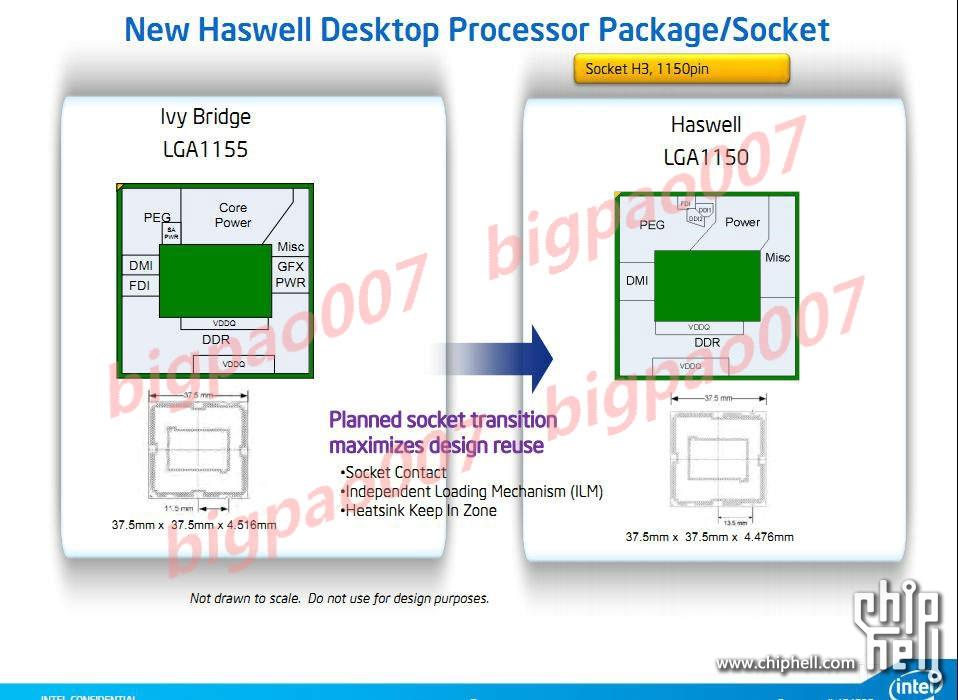
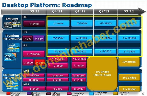
Ivy Bridge-E in Q4 2012, Compatible with LGA2011 and X79

Earlier this week, Intel launched the fastest desktop processors under its Core i7 "Sandy Bridge-E" platform, with is partners, motherboard, memory and cooler vendors. Less than a week into its shelf life, Sandy Bridge-E already has a successor taking shape at Intel, slated for the fourth quarter of 2012, but that's far from being the most interesting part of this news. According to a new internal slide scored by a source at XFastest, Ivy Bridge-E will be compatible with today's Intel X79 platform, and LGA2011 socket.

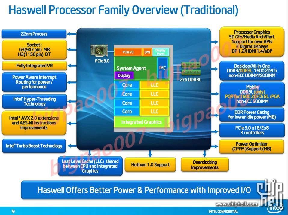
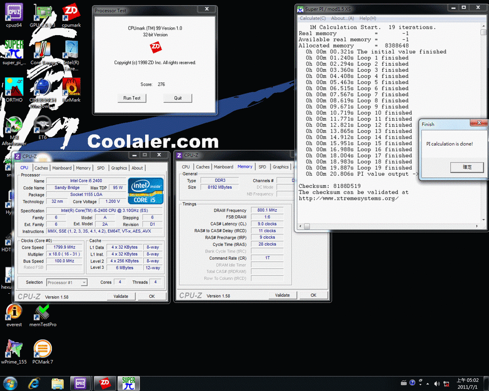
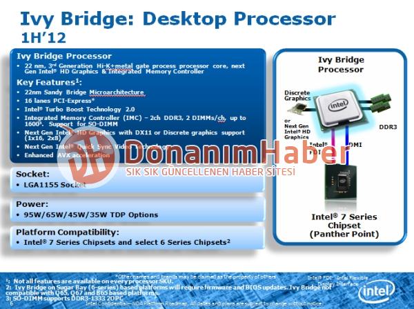
Suddenly, Sandy Bridge-E makes for a sweeter deal because its platform longevity (for upgrades) is at least two years. Ivy Bridge-E, like Ivy Bridge LGA1155, will be built on the 22 nanometer silicon fabrication process. We don't expect Ivy Bridge-E to be much more than an optical shrink of today's Sandy Bridge-E silicon, but the shrink could leave scope for enabling some of its components otherwise locked out for the Core processor family. Sandy Bridge-E silicon physically holds 8 cores and 20 MB of L3 cache, but the fastest Core processor based on it has just 6 of those cores, and 15 MB of L3 enabled. The source at XFastest says that while Ivy Bridge-E is slated for Q4 2012, the LGA1155 Ivy Bridge will launch across Q1 and Q2 of 2012 (March~April).

All's Well That Haswell?

Here are the first slides detailing Haswell, Intel's next generation processor architecture that succeeds Sandy Bridge and Ivy Bridge. Intel follows a "tick-tock" product development model. Every year, Intel's product lineup sees either of the two. A "tock" brings in a new x86 architecture, a "tick" miniaturizes it to a newer silicon fabrication process. For example, Sandy Bridge is Intel's latest architecture, and is based on the 32 nm fab process. Ivy Bridge is a miniaturization of Sandy Bridge to 22 nm. Likewise, Haswell will be a brand new architecture, it will use the 22 nm fab process cemented by Ivy Bridge.

If all goes well with Intel's 22 nm process, Haswell is scheduled for Q2 2013. 2012 (Q2 onwards) will be led by Ivy Bridge. But then here's a "shocker": Haswell's desktop version will use a brand new socket, LGA1150, and will be incompatible with LGA1155. This is because of drastic changes in the pin map of the package. Sandy Bridge and Ivy Bridge share the LGA1155 socket, and will hence, have kept the socket alive for over 2 years. A major change with the component arrangement in the platform that is affecting Haswell's pin map is that Haswell will have a higher bandwidth chipset bus, rearranged PCIe pins (with FDI pins), rearranged power pins, and miscellaneous pins. It does away with a separate power domain for the integrated graphics controller.

Are Improving Integrated Graphics Slowly Killing Off Discrete Graphics Cards?

Intel started the trend of improving integrated graphics with their second generation LGA1155 socket Core i3, i5 & i7 line of processors. Depending on the model, these processors sport integrated HD2000 or HD3000 graphics right on the processor die, which nowadays give acceptable performance for low-end gaming and can play Full HD 1080p video perfectly. This trend is increasing with the upcoming Ivy Bridge processors, which will be able to support a massive 4096 x 4096 pixel display, as we reported here. AMD now also have equivalent products with their Llano-based A-series processors. So, where does this leave discrete graphics cards? Well, the low end market is certainly seeing reduced sales, as there really isn't enough of a performance difference nowadays to always warrant an upgrade from an IGP. As integrated graphics improve further, one can see how this will hurt sales of higher end graphics cards too. The problem is that the bulk of the profit comes not from the top-end powerhouse graphics cards, but from the low to mid-end cards which allow these companies to remain in business, so cannibalizing sales of these products to integrated graphics could make high-end graphics cards a much more niche product and crucially, much more expensive with to boot.

Ivy Bridge Quad-Core to Have 77W TDP, Intel Plans for LGA1155 Ivy Bridge Entry

Intel's next generation "Ivy Bridge" Core processors slated for 2012 will mark the beginning of Intel's transition to the brand new 22 nanometer fab process. It looks like Ivy Bridge will significantly benefit from this transition, since Intel will raise the bar in terms of energy-efficiency. Even the fastest P1 (performance 1) tier quad-core chips will have TDP rated as low as 77W, down from the 95W Core i7 2600K, for example, has.

The punters at Intel marketing have sliced the market down to finer segments, to better address it. The market is sliced in terms of price-segments (vertical), and in terms of target users (horizontal). The two markers are independent of each other, yet they complement each other in pin-pointing areas of the market Intel can address. Ivy Bridge LGA1155 is restricted to P1 (performance tier 1) segment on the top, with higher tiers, along with HEDT (high-end desktop) being reserved for Sandy Bridge-E LGA2011, and future "Ivy Bridge-E". Horizontally, Intel will have "K" quad-core parts for Enthusiast, standard (locked) quad-core vPro for the Standard, "T" quad-core for Performance-optimized lifestyle, and "S" for Power-optimized lifestyle. Chaotic as it looks, the table below lays out the lineup perfectly.

ASUS Unveils ROG Maximus IV Gene-Z/Gen 3 with PCI-Express 3.0 Slots

ASUS is ready with a new PCI-Express 3.0 compliant socket LGA1155 motherboard, adding to its recently-launched line of Intel Z68 chipset-based boards that feature Gen 3.0 PCI-Express x16 slots. This latest one is part of the elite Republic of Gamers (ROG) family, and is built on the compact micro-ATX form factor, called Maximus IV Gene-Z/Gen 3. This is the second modification of the Maximus IV Gene, the original was based on Intel P67 chipset, the Gene-Z replaced the chipset with Intel Z68 that supports Smart Response technology, while the Gene-Z/Gen 3 adds PCI-Express 3.0 x16 slots.

The board uses a 12-phase Digi+ VRM for the CPU, it is wired to four DDR3 DIMM slots supporting DRAM speeds of up to DDR3-2200 MHz with overclocking. The socket is wired to two PCI-Express 3.0 x16 slots over Gen 3 compliant switches and electrical components, the slots configure to PCI-Express 3.0 x8/x8 when both are populated. PCI-Express Gen 3 support requires next-generation 22 nm Ivy Bridge Core processors, which will be launched next year. The only other expansion slot is an open-ended PCI-Express 2.0 x4, wired to the Z68 PCH. NVIDIA SLI and AMD CrossFire are supported.

Sandy Bridge-E VT-d Broken In C1 Stepping, Fixed In C2 Stepping, Shortly After Launch

PC enthusiast customers and companies running corporate datacentres looking to buy into the new Sandy Bridge-E platform may want to wait a little while before handing over their hard-earned money to Intel. The initial batch of C1 revision Sandy Bridge-E processors have a bug - "errata" in Intel terminology - in them with VT-d, which means that hardware accelerated virtualization doesn't work properly with them (software only mode is unaffected). The feature when working properly, allows all hardware acceleration to work on the hosted operating system (virtual machine). This would allow things such as hard drive controllers to work, plus applications such as high-powered 3D games, typically First Person Shooters, to run at nearly full speed and the full Windows Aero desktop to be displayed on the hosted OS, as the hardware features of the graphics card can be used. Therefore, working VT-d is a critical feature for these kinds of applications.

Super-High 4096 x 4096 Display From An IGP? The Upcoming Ivy Bridge Can Do It

The new Ivy Bridge processors, due out in about six months, have one apparently overlooked but important feature. No, it's not the greatly increased speed (about double or more of Sandy Bridge) or the advanced feature set. It's actually the super-high resolution capability: specifically 4096 x 4096 pixels. This astonishing capability is far better than any of the top-end discreet graphics cards such as the NVIDIA GTX 590 or AMD HD 6990 via a single monitor port. It's so high in fact, that there's almost no content at that resolution and no monitor that can handle it. This IGP can actually play multiple 4K video streams, too. NVIDIA unsurprisingly, is talking up the gaming possibilites at such a resolution. I'd like to see what kind of monster GPU could handle it. It will be interesting to see what uses this capability gets put to generally - and just how much the whole setup will cost.

Gigabyte Responds to MSI's Bluff Call

A little earlier this month, MSI's PR team dished out a presentation in which they claimed that Gigabyte was misleading buyers into thinking that as many as 40 of its recently-launched motherboards were "Ready for Native PCIe Gen.3". MSI tried to make its argument plausible by explaining what exactly goes into making a Gen 3-ready motherboard. The presentation caused quite some drama in the comments. Gigabyte responded with a presentation of its own, in which it counter-claimed that those making the accusations ignored some key details. Details such as "what if the Ivy Bridge CPU is wired to the first PCIe slot (lane switches won't matter)?"

Gigabyte Announces Ultra Durable 4 Motherboard Construction Technology

Gigabyte is one of the oldest motherboard manufacturers that made component choice, PCB construction, and the resulting durability as a selling point, with its Ultra Durable moniker. Each succeeding version of Ultra Durable denotes a higher grade of durability, with the introduction of newer classes of components that add to the durability. Ultra Durable started off as denoting motherboards with all Solid-state capacitors (conductive polymer), that are more durable compared to electrolytic ones. Ultra Durable 2 upped it with Ferrite Core chokes that have lower energy loss to noise and head, and lower resulting RDS(on) MOSFETs. Ultra Durable 3 further upped that with a PCB that has additional copper layers that help improving signalling, grounding, and cooling.

Today, Gigabyte added the fourth version of Ultra Durable, that addresses more elements that threaten the durability of a motherboards. Ultra Durable 4, as it's called, is a set of technologies that are layered on top of Ultra Durable 3, and addresses the problems of humidity, electrostatic discharge, high temperature, and power surge. Humidity is a natural element, moisture eats into components that have pure metals such as aluminum and copper, over time. Electrostatic discharge has a devastating impact on sensitive electronics, while power surges, usually caused after recovery from a power outage, can fry power conditioning electronics of the motherboard. And then we all know what high-temperature can do to tiny capacitors and FETs.

Intel Desktop Board Lineup for 2011-12 Disclosed

Here are some of the first motherboards by Intel's Desktop Board brand of consumer motherboards. Towards the end of 2011, Intel will release its Sandy Bridge-E high-end desktop platform. Like with the launch of any new chipset or desktop platform, Intel will have its Desktop Board products in place, that follow the chipset and branding specifications to the letter. With Sandy Bridge-E, Intel will launch two Extreme Series motherboards, the DX79SI and the DX79TO. In the second half of 2011, Intel will also launch a variety of Intel Atom boards, including one codenamed "Marshaltown".

Then in the first half of 2012, Intel will launch its next-generation 22 nm "Ivy Bridge" desktop processors in the LGA1155 package (compatible with Sandy Bridge). To back its launch, Intel will release a new chipset called Z77 Express. There will be no discrete graphics chipsets. H77 is the client desktop chipset that lacks overclocking features. Z77 has them, and support for Smart Response technology. Q77 adds a few enterprise management features. Intel's Z77 based motherboards include two Extreme series models, and two top-end Media Series models.

Sandy Bridge-E 2011 Launch Put on Slide, Ivy Bridge in March-April 2012

Last month, there reports of Intel pushing its Sandy Bridge-E enthusiast desktop platform to 2011. It was originally scheduled for 2011, but was reportedly delayed to 2012 because of issues Intel was facing with its flagship desktop chipset, codenamed Patsburg-D. Intel will be launching Sandy Bridge-E this year, but the first wave of motherboards will feature Patsburg-A/B chipsets, which have fewer SATA 6 Gb/s ports than Patsburg-D.

Intel put its launch plans on paper with its latest desktop platform roadmap, that shows the first three models of socket LGA2011 Sandy Bridge-E processors, the six-core Core i7-3960X, Core i7-3930K, and the quad-core Core i7-3820, featuring in the Q4 2011 column. The roadmap shows that the three processors will hold their market-positions till Q2-2012, when Intel will release faster models to displace them. The roadmap slide also shows that Ivy Bridge, Intel's next-generation socket LGA1155 processors that are built on the 22 nm fab process, will be released in March or April 2012, and not early 2012 as speculated earlier.

Production Gigabyte G1.Sniper 2 Features PCI-Express Gen. 3

About a month ago, we were treated to the first pictures of G1.Sniper 2, Gigabyte's first LGA1155 motherboard in its G1.Killer series of motherboards targeting the gamer-overclocker market segment. High resolution pictures showed the prototype of having PCI-Express Gen. 2 slots like most other LGA1155 boards. It turns out, according to a photo-session of a production sample by tech-blog SIN's Hardware, that Gigabyte refined the design with the production version (the one that will be sold in the markets), it features PCI-Express 3.0 (Gen. 3) graphics slots.

For a LGA1155 motherboard to have Gen. 3 PEG slots, it requires Gen. 3 specifications compliant switching circuitry, which wasn't available to motherboard vendors when they were designing their first LGA1155 boards. With availability of those components, motherboard vendors are not wasting any time in rolling out new variants of their LGA1155 boards that feature Gen. 3 PCI-Express slots. Gigabyte placed "PCI-Express 3.0" marking on the board manually using stickers, going on to show that adding Gen. 3 slots indeed may have been a last-minute decision at Gigabyte. The other interesting marking on the G1.Sniper 2 carton is the mention of the board being ready for upcoming 22 nm "Ivy Bridge" Core processors. More pictures, and a preview at the source.

Intel Aims at 10 nm Processors by 2018

It's not just host nations of the Olympics that are decided almost decades in advance, but also Intel's silicon names and the fab process they're going to be built on. Intel has its plan for the greater part of this decade already charted out, well beyond the upcoming Ivy Bridge architecture. Intel follows the "tick-tock" product cycle, where every micro-architecture gets to be built on two succeeding fab processes, and every fab process getting to have two succeeding micro-architectures built on it, in succession. Westmere is an optical shrink of the Nehalem architecture, it was a "tick" for the 32 nm process, Sandy Bridge is its "tock", and a new architecture. Ivy Bridge is essentially an optical shrink of Sandy Bridge, it is the "tick" for 22 nm process.

Ivy Bridge will make its entry through the LGA1155 platform in 2012, it will make up the 2012 Core processor family. Haswell is the next-generation architecture that succeeds Sandy Bridge and IvyBridge, it will be built on the 22 nm process, and is expected to arrive in 2013. Roswell is its optical shrink to 14 nm, slated for 2014. Looking deep into the decade, there's Skylake architecture, that will span across 14 nm and 10 nm processes with Skymont. This model ensures that Intel has to upgrade its fabs every 2 or so years, an entirely new micro-architecture every 2 or so years as well, while providing optical shrinks every alternating year. Optical shrinks introduce new features, increased caches, and allow higher clock speeds. 10 nm for processors by 2018 sounds realistic looking at the advancement of NAND flash technologies that are pushing the boundaries of fab process development. NAND flash is much less complex than processor development, and hence serve as good precursors to a new process.

ZOTAC Readies Monster LGA1155 Motherboard

ZOTAC entered the motherboard scene as yet another vendor of reference NVIDIA nForce motherboards, which the like of EVGA, XFX, and BFG also sold. After the fall of nForce, ZOTAC attempted a LGA1366 motherboard, and went dormant with motherboards. Later, it picked up interest in the mini-ITX form-factor as it gained popularity in Asian markets like China and India, manufacturing motherboards based on Intel Atom, Atom with NVIDIA ION, and eventually socketed mini-ITX motherboards as it became a 2-chip affair with Intel's Ibex Peak platform (LGA1156). It looks like Zotac is making a comeback into full-size ATX motherboards that target the very top tier of the market, to woo gamers, professional overclockers, and enthusiasts.

Seen here is what the Chinese press is referring to as "ZT-Z68 Crown Edition-U1DU3", we may have lost the correct name in translation, but let's call it ZT-Z68-U1DU3 for now. It is a full-size ATX motherboard that takes socket LGA1155 Intel Sandy Bridge and future Ivy Bridge processors, and is based on the Intel Z68 Express chipset. It combines a strong VRM to support extreme overclocking, with graphics expansion, adding 4-way NVIDIA SLI and AMD CrossFireX capabilities using an NVIDIA BR-03 bridge-chip that sits on the processor's PCI-E x16 link, to give out two PCI-Express 2.0 x16 links, which are then spread between four slots in x16/NC/x16/NC, x16/NC/x8/x8, or x8/x8/x8/x8 lane configurations.

Intel Ivy Bridge Dual-Core Put Through Clock-to-Clock Benches Against Sandy Bridge

Taiwanese PC enthusiast Coolaler has a new Ivy Bridge LGA1155 dual-core engineering sample to play with, and wasted no time in putting it through some tests. The sample has two cores, four threads with HyperThreading enabled, clock speed of 1.80 GHz, 256 KB L2 cache per core, and 4 MB shared L3 cache. It is running on an Intel P67 chipset-based motherboard with 8 GB of dual-channel DDR3-1600 MHz memory. At 1.80 GHz, it may not be game for absolute performance figures since it's unlikely that Intel will release a chip with that clock speed unless it has unreal performance:clockspeed gains over Sandy Bridge; but it's good enough for clock-to-clock performance comparisons between Ivy Bridge and Sandy Bridge. A Core i5-2400 was clocked at 1.80 GHz with 18x BClk multiplier, and put through a single-threaded benchmark, and a multithreaded one.

The cache and memory benchmark that measures bandwidth and latency of caches and memory was unable to measure bandwidth, but measured some latencies. The L1 cache at 2.2 nanoseconds (ns), and L2 at 2.9 ns. Next, the Ivy Bridge DC, and the Core i5-2400 (@ 1.80 GHz) testbeds were put through CPUMark 99, where Ivy Bridge DC scored 278 points, and Core i5-2400 clocked at 1.80 GHz scored closely followed at 276 points. Moving on to multithreaded performance, the two were put through Cinebench 11.5 64-bit. The Ivy Bridge DC chip scored 1.81 points; while the Core i5-2400 clocked at 1.80 GHz, scored 2.61 points. Coolaler promises more benches.

ASRock Readies Z68 Fatal1ty Motherboard with PCI-Express 3.0 Slots

ASRock gave its premium LGA1155 motherboard lineup a boost with the new Z68 Fatal1ty. Apart from being a Z68 chipset based motherboard modeled along the lines of its predecessor, the ASRock P67 Fatal1ty, the new motherboard features PCI-Express 3.0 graphics slots, that work on Sandy Bridge and future Ivy Bridge processors. The new third generation PCI-E interconnect can drive 1 GB/s of data per link, per direction. You'll need PCI-E 3.0 compliant add-on cards to make use of that bandwidth, current graphics cards will run at Gen. 2 speeds. One advantage here could be that AMD Radeon HD 5000 and HD 6000 series single-GPU graphics cards will run on Gen 2.1 mode, which has slightly higher bandwidth at its disposal thanks to its lower-overhead data coding scheme.

The ASRock Z68 Fatal1ty is designed for both gamers and overclockers, using high-grade components. The LGA1155 socket is powered by a 18-phase VRM, wired to four DDR3 DIMM slots supporting dual-channel DDR3-2133 MHz (Ivy Bridge IMC's optimal memory speed). Featuring Intel Flexible Display Interface (FDI), the board allows you to use the integrated graphics. With the Lucid Virtu technology, you can switch between the integrated graphics, and discrete graphics cards. Expansion slots include two PCI-Express 3.0 x16 (electrical x8/x8 when both are populated), one PCI-Express 2.0 x16 (electrical x4, wired to Z68 PCH), and two each of PCI-E 2.0 x1 and legacy PCI.

ZOTAC Z68-ITX WiFi a Fun-Sized Treat for Overclockers

Rarely do motherboard vendors dish out mini-ITX form-factor motherboards targeting the overclocking community. There's little space to squeeze in the bare essentials, but nothing is impossible, if there are competent designers at work, a case in point is the new Z68-ITX WiFi from ZOTAC. Based on the Intel Z68 Express chipset, this board supports LGA1155 Core i3/i5/i7 Sandy Bridge, and future Ivy Bridge processors, supports their integrated GPU giving you access to Intel QuickSync technology, as well as a suite of overclocking options.

To begin with the LGA1155 socket is powered by an 8-phase digital-PWM power design that uses high-grade PWM chokes made by Pulse, and in all probability, a Volterra PWM IC giving you precise voltage control as well as vDroop protection (high-precision load-line calibration). It also uses server-grade high-C capacitors. The PWM circuit takes input from an 8-pin EPS connector. The PWM chips are cooled by a large heatsink that sends some of its heat to the heatsink cooling the Z68 PCH, over a heat pipe.

MSI New Z68A-GD80 Swims in PCI-Express 3.0 Fame

While Sandy Bridge-E LGA2011 processors will come with integrated PCI-Express 3.0 hubs, they're still a couple of quarter financial years away. Meanwhile, MSI jumped the gun on its latest socket LGA1155 Intel Z68-based motherboard with not only support for Intel's upcoming 22 nm Ivy Bridge LGA1155 processors, but also the PCI-Express 3.0 hubs that the new processors come with. While Ivy Bridge has PCI-E 3.0 hub, not just any LGA1155 motherboard can give you PCI-E 3.0 support. It requires slots that are compliant with the new specification, and needs PCI-E 3.0 compliant external switching chips. MSI has both, on its new Z68A-GD80 motherboard, and with it, the bragging rights of being the world's first PCI-E 3.0 compliant motherboard.

PCI-Express 3.0 gives you twice the interface bandwidth as PCI-Express 2.0, which means that PCI-Express 3.0 x8 has the same bandwidth as PCI-Express 2.0 x16. But before you celebrate, let's remind ourselves that you also need a PCI-E 3.0 compliant GPU to make the slots operate at Gen 3.0 speeds. Installing PCI-Express 2.0 GPUs on Gen 3.0 won't run the slots at Gen 3.0 speeds. That aside, the Z68A-GD80 is a sufficiently-equipped enthusiast motherboard featuring 14-phase VRM for the CPU, dual-channel DDR3-2133 support, two PCI-E 3.0 x16 slots (x8/x8 with populated), a third PCI-E x16 wired to the Z68 PCH, running at PCI-E 2.0 x4 speeds, and a couple of PCI-E 2.0 x1 and legacy PCI. There are three internal SATA 6 Gb/s ports; eSATA, USB 3.0, make for the rest of the connectivity. There is full-fledged display connectivity, with Lucid Virtu support. Expect this board to be out any time soon.

Intel Reinvents Transistors Using New 3-D Structure

Intel Corporation today announced a significant breakthrough in the evolution of the transistor, the microscopic building block of modern electronics. For the first time since the invention of silicon transistors over 50 years ago, transistors using a three-dimensional structure will be put into high-volume manufacturing. Intel will introduce a revolutionary 3-D transistor design called Tri-Gate, first disclosed by Intel in 2002, into high-volume manufacturing at the 22-nanometer (nm) node in an Intel chip codenamed "Ivy Bridge." A nanometer is one-billionth of a meter.

The three-dimensional Tri-Gate transistors represent a fundamental departure from the two-dimensional planar transistor structure that has powered not only all computers, mobile phones and consumer electronics to-date, but also the electronic controls within cars, spacecraft, household appliances, medical devices and virtually thousands of other everyday devices for decades.

Intel Smart Response Technology Detailed

Remember the very first strains of Ibex Peak LGA1156 platform motherboards such as this one? Remember that small memory slot next to the bigger DIMM slots? That was Intel's ambitious "Braidwood" technology, a NAND-flash based hard drive assist feature. Fast NAND flash memory would be installed onto the motherboard in the form of removable modules, and those modules would quicken system booting, and act as a fast cache for the system drive. Alas, Braidwood was axed for reasons unknown till date. Maybe it made Ibex Peak platform a lot faster than it should be, or maybe its design wasn't perfected or flawed. Regardles, it disappeared.

Two platforms (Ibex Peak and Cougar Point) later, a similar technology is making its way through Intel's pipes, this time it has a proper market name: Intel Smart Response Technology, and comes with another new development, Larsen Creek. Larsen Creek is the codename of Intel's upcoming line of solid state drives. However, it is targeting entry-level, low-capacity markets, and what better way to sell it than club it with Intel's new platform technology, Smart Response. Instead of NAND flash modules (Braidwood), Intel's Smart Response technology uses SATA SSDs to accelerate hard drives. The SSD can be of any size and speed, it's just that Larsen Creek is the most appropriate given that it will come in capacities as low as 20 GB, and be quite inexpensive.

Ivy Bridge CPUs Feature PCI-Express 3.0

Slides detailing Intel's upcoming "Panther Point" chipset reveal that the next generation of LGA1155 processors will feature PCI-Express 3.0 bus to connect with graphics cards. PCI-Express 3.0 doubles bandwidth over PCI-Express 2.0, and comes with a number of new features and electrical specifications. With Panther Point, Intel put an end to chipsets meant for discrete graphics (such as P67). Here on, all LGA1155 chipsets will support Intel Flexible Display Interface (FDI), although only the Z-series will support overclocking. Among the Z-series, Z77 is the top part supporting a wider range of PCI-Express configurations, Z75 supports discrete graphics with up to 2 graphics cards, while H77 only supports one graphics card, and lacks overclocking features.

Unlike the X79 LGA2011 chipset, Panther Point chipsets don't feature massive 10-port SATA 6 Gb/s storage controllers. Like Cougar Point, it features two SATA 6 Gb/s ports, and four SATA 3 Gb/s. The chipset embeds a USB 3.0 controller, but only 4 out of 14 USB ports are USB 3.0, rest are USB 2.0. Intel's Ivy Bridge will make for the company's 2012 Core Family portfolio, supplying entry-thru-performance segments with processor, while enthusiast segment is care of a different platform.

Intel Ivy Bridge Feature Set Detailed

Some time in the first half of 2012, Intel will release its next generation of desktop processors for the LGA1155 socket, based on the new Ivy Bridge silicon. Ivy Bridge is a 22 nanometer die-shrink of Sandy Bridge, with a few features added/improved. Ivy Bridge's smaller die size will allow for increased clock speeds and reduced production costs. A presentation was leaked to the press, which reveals quite a bit about the new chips. To begin with, Ivy Bridge processors are seamlessly compatible with existing LGA1155 platforms, and "Cougar Point" P67, H67, H61, Z68, chipsets, although it will come with its own 7-series chipset.

For the most part, Ivy Bridge is identical to Sandy Bridge, being an optical shrink from existing 32 nm to 22 nm. It will feature a new dual-channel DDR3 memory controller with official support for DRAM speeds of up to DDR3-1600 MHz. There's the usual PCI-Express 2.0 x16 hub that can drive up to two discrete graphics cards with electrical x8 connections. The integrated graphics controller will face an overhaul, it will be DirectX 11 compliant. It will also support the next version of Intel QuickSync GPU-accelerated video encoding technology. Turbo Boost 2.0 will be carried forward. TDP ranges in the usual 95/65/45/35W options.

Intel Accelerating Ivy Bridge Unveiling to Computex 2011

Intel is preparing to unveil its next-generation processors based on the Ivy Bridge architecture as early as by Computex 2011 (May 30 to June 4), according to Commercial Times, a Chinese language business newspaper. Ivy Bridge is an optical shrink of the Sandy Bridge architecture, processors based on it will be manufactured on the 22 nanometer silicon fabrication process. Intel launched its Sandy Bridge 32 nm processors at CES 2011, in January. In related news from the same source, AMD has also accelerated the production of its Llano APUs and is expected to begin shipping the APUs to ODM/OEM makers in May at the earliest instead of the original schedule set in the third quarter.
Return to Keyword Browsing
Apr 25th, 2024 01:56 EDT change timezone

New Forum Posts

Popular Reviews

Controversial News Posts