News Posts matching #Kepler

Return to Keyword Browsing

Next-Gen. Razer Blade Combines Ivy Bridge and Kepler

Even as the Razer's first gaming notebook, the Blade, has the guts to command a US $2,800 price for its dual-core processor and GeForce GT 555M graphics, which still went on to sell-out, according to its makers, its successor is already taking shape, suggests a BSN report. The next-generation Blade notebook is said to combine an Intel Core processor based on the 22 nm "Ivy Bridge" architecture, with NVIDIA's exciting new 28 nm graphics based on the Kepler architecture. The Razer Blade is what its makers claim to be "the world's first true gaming laptop."

New NVIDIA GeForce GTX 680 Pictures Hit The Web

Courtesy of ChipHell we now have a couple of fresh pictures of NVIDIA's first Kepler-powered graphics card, the GeForce (or should we write' GeFORCE') GTX 680. Shot both from above and the back, the incoming card has a black PCB, a dual-slot/single-fan cooler, two (stacked) 6-pin PCIe power plugs, a couple of SLI connectors, and four display outputs - dual DVI, HDMI and DisplayPort.

The GTX 680 is equipped with one GK104 28 nm GPU, and reportedly boasts 1536 CUDA Cores, a 256-bit memory interface, 2 GB of GDDR5 VRAM (4 GB models should also be in the works), PCI-Express 3.0, and a TDP of around 190 W. The GeForce GTX 680 is expected to be launched next week, on March 22nd. Its rumored price tag is $549.

More Pictures of GK104 Reference Board Surface

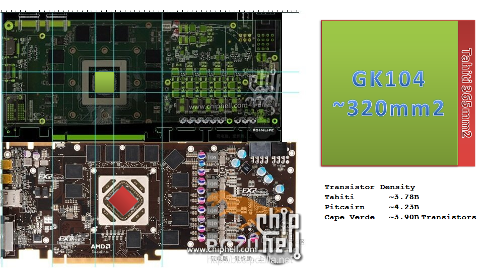
Here is a brief compilation of all the new images of the upcoming NVIDIA GeForce Kepler high-performance product, which our forum members posted through the day. The pictures reinforce the 3QTR picture that surfaced this Thursday, and full-length picture of the PCB that 
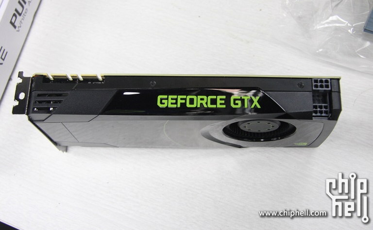
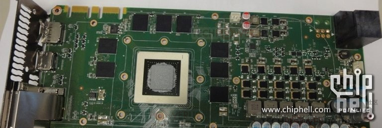
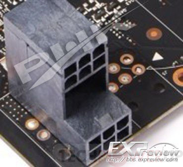
surfaced earlier this month. The first picture below, reveals what is essentially the card that was pictured yesterday, with its cooler shroud taken out. You will find a conventional air-channel cooler design. A lateral-flow fan, which looks similar to the one used in GeForce GTX 580/570), directs air through a dense aluminum channel array, which draws heat from key components such as the GPU, memory, and VRM, using a vapor-chamber plate (again, similar to the one used on high-end GeForce GTX 500 series). Towards the rear portion, you'll spot the piggy-backed 6+6-pin PCIe power connector cluster. You will also find the black rugged metal base-plate flowing along the full length of the PCB, structurally reinforcing it, and performing some cooling functions.

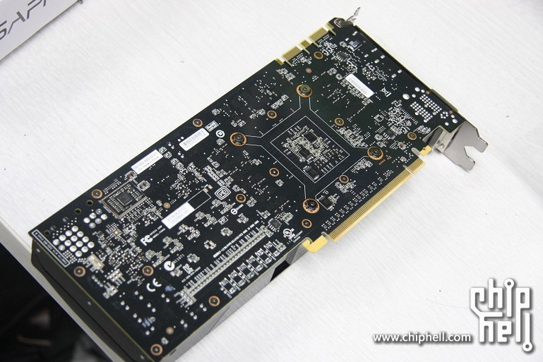
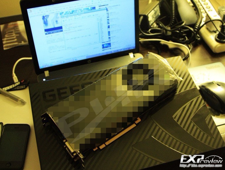
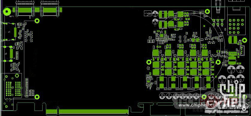
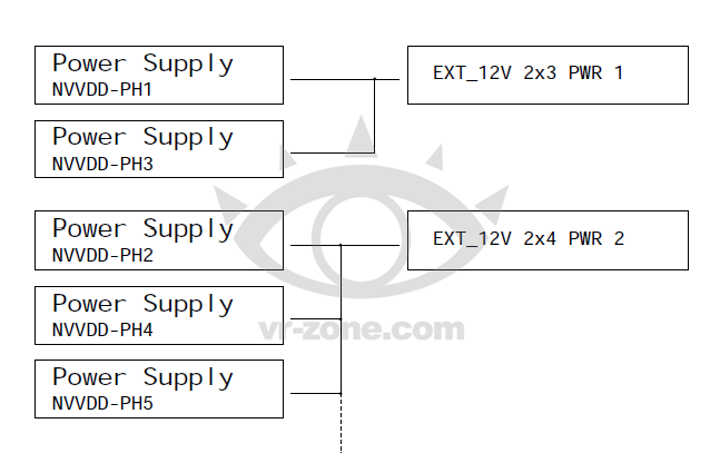
Moving on, the second picture reveals the same VRM area we saw earlier, on the green-colored PCB engineering sample, with its five NVVDD phases. The third picture is the first, of the reverse side of the PCB. Revealing most of the solder points, and electrical circuitry. The driver ICs of each of the NVVDD phases can be seen here. These two pictures confirm that the retail version of the GK104 product will feature a black PCB (the brown tinge is natural, due to the dense network of traces and ground layers, made of copper). The fourth picture reveals what looks like NVIDIA's Media Kit. Reputed reviewers get a NVIDIA-branded "media kit", which contains the graphics card sample to review, and other relevant documentation in printed form, along with a driver CD, and other accessories. These cards are not branded by any AIC partner, and are 100% compliant to NVIDIA's reference design and clock speeds.

Many Thanks to our community members JaredPace and CrapDaddy.

Acer VA40 Combines Core i7-3612QM and GeForce GT 640M

NVIDIA's Kepler and Intel's Ivy Bridge architectures are a match made in Acer's upcoming VA40 notebook. The notebook combines Intel Core i7-3612QM quad-core processor with NVIDIA GeForce GT 640M discrete graphics, and with NVIDIA Optimus technology, performs dynamic-switching between the GT 640M and Intel HD 4000 graphics embedded into the processor. A Chinese forum user "yknyong1" posted screenshots of the two components using available diagnostic software. We know that CPU-Z 1.6 adds reliable support for Ivy Bridge CPUs, but GPU-Z 0.5.9 has preliminary support for Kepler GPUs, too. At least it knows how to count CUDA cores, ROPs, clock-speeds, and other basic information, even if it gets a few other details inaccurate. Kepler support will be refined and made reliable days ahead of NVIDIA's big launch day, later this month.

The Core i7-3612QM is a quad-core chip clocked at 2.10 GHz, featuring 6 MB L3 cache of the Ivy Bridge silicon, and HyperThreading, which enables 8 logical CPUs. The GeForce GT 640M, on the other hand, is known to be based on NVIDIA's new 28 nm GK107 silicon. It is detected with 384 CUDA cores, 2 GB of DDR3 memory over a 128-bit wide memory interface, 16 ROPs, core clock speed of 405 MHz, and 900 MHz memory. The chip carries a device ID of 10DE-0FD2, and is compliant with PCI-Express 3.0 bus interface. When on light load (desktop), the clock speeds of this GPU were turned down to 135 MHz core with 405 MHz memory. Find more barely-legible screenshots at the source.

GK104 Dynamic Clock Adjustment Detailed

With its GeForce Kepler family, at least the higher-end parts, NVIDIA will introduce what it calls Dynamic Clock Adjustment, which adjusts the clock speeds of the GPU below, and above the base-line clock speeds, depending on the load. The approach to this would be similar to how CPU vendors do it (Intel Turbo Boost and AMD Turbo Core). Turning down clock speeds under low loads is not new to discrete GPUs, however, going above the base-line dynamically, is.

There is quite some confusion regarding NVIDIA continuing to use "hot clocks" with GK104, the theory for and against the notion have been enforced by conflicting reports, however we now know that punters with both views were looking at it from a binary viewpoint. The new Dynamic Clock Adjustment is similar and complementary to "hot clocks", but differs in that Kepler GPUs come with a large number of power plans (dozens), and operate taking into account load, temperature, and power consumption.

GK104 Graphics Card Pictured?

Could this be the very first picture of NVIDIA's GeForce Kepler 104-based graphics card? This Mr. Blurrycam shot has been doing rounds in Chinese forums. While it may not seem convincing at first glance, several features of the card in the picture seem to match the layout of the GK104 reference PCB which was pictured, earlier. To begin with, on the top-right corner you can train your eyes to a deep cutout, for the unusual piggy-backed 6+6 pin PCIe power connectors. The rear panel bracket is a 100% match (in layout and design of exhaust vents), of the one with the true-color image of the GK104 PCB. The only feature that clouds the plausibility of this picture is "GeForce GTX 670 Ti" being etched onto the cooler's shroud. We're hearing more voices refer to the top GK104 part as "GeForce GTX 680" than "GTX 670 Ti". We're also hearing that NVIDIA will adopt a new GeForce logo, so that glaring "GEFORCE" badge on the top of the card looks plausible.

UPDATE: Added less blurry picture.

Epic's UE3-Powered Samaritan Demo Showcased Running on NVIDIA Kepler Card

One year after its debut, Epic Games' Samaritan Tech Demo is back at the GDC (Game Developers Conference) and it's there to tease the power of NVIDIA's Kepler 28 nm GPU. At last year's GDC Samaritan, which is based on Unreal Engine 3, was running in real-time on three GeForce GTX 580 cards set in SLI. This year Epic is showing off the demo running on a single NVIDIA Kepler graphics card.

GeForce GTX 680 Features Speed Boost, Arrives This Month, etc., etc.

Here are some key bits of information concerning the upcoming GeForce GTX 680, a performance single-GPU graphics card based on the 28 nm GK104 GPU by NVIDIA. The information, at face value, is credible, because we're hearing that a large contingent of the media that finds interest in the GPU industry, is attending the Game Developers Conference, where it could interact with NVIDIA, on the sidelines. The source, however, is citing people it spoke to at CeBIT.

First, and most interesting: with some models of the GeForce 600, NVIDIA will introduce a load-based clock speed-boost feature (think: Intel Turbo Boost), which steps up clock speeds of the graphics card when subjected to heavy loads. If there's a particularly stressing 3D scene for the GPU to render, it overclocks itself, and sees the scene through. This ensures higher minimum and average frame-rates.

Toshiba Qosmio X870 Detailed

Here's a picture of Toshiba's its newest gaming notebook in the works, the Qosmio X870. Although unveiled, it will be a little while before we can see this 17.3-incher in stores. That's because it's said to powered by "next-generation" Core processors (Ivy Bridge), and "next-generation" NVIDIA GeForce GPU (Kepler), with 3 GB of GDDR5 memory. Its 17.3-inch TruBrite display packs 1920x1080 pixels resolution. Other notable specifications of this brute includes 2TB SSD+HDD hybrid, Bluetooth 4.0, four USB 3.0 ports, Harman-Kardon speakers, Blu-ray drive, and wired Ethernet. According to the source, the Qosmio X870 is headed for a Q2-2012 launch.

GeForce GTX 680 Final Clocks Exposed, Allegedly

Waiting on Kepler before making a new GPU purchase? Well, you have to wait a little longer. Thankfully, this wait can be eased with the latest leaks about NVIDIA's 28 nm chip and the GeForce GTX 680 it powers.

According to VR-Zone, the GTX 680 does indeed feature 1536 CUDA Cores and a 256-bit memory interface, but it also has hotclocks, meaning the GPU is set to 705 MHz but the shaders operate at 1411 MHz. The memory (2 GB most likely) is supposed to be clocked at 6000 MHz giving a total memory bandwidth of 192 GB/s.

NVIDIA's incoming card is 10 inches long and also has 3-way SLI support, and four display outputs - two DVI, one HDMI and one DisplayPort. The GeForce GTX 680 is expected to be revealed on March 12 and should become available on March 23rd.

GK104 Die-Size Estimated

Thanks to some good understanding of geometry, and great Photoshop skills, the punters have estimated the die-size of NVIDIA's GeForce Kepler 104 (GK104) GPU, using a picture of the NVIDIA reference board that was leaked last week. Compared to the known die-size of an AMD "Tahiti"-based graphics card, the die-size of GK104 was estimated to be around 320 mm², about 45 mm² smaller than Tahiti. The relative transistor density of the chip, compared to AMD's 28 nm chips, were also estimated.

GK104 PCB Pictured in Full

Here is the first true-color picture of the GeForce Kepler 104 (GK104) reference PCB shot in full (well, almost, excluding the uneventful PCIe bus connector). The picture provides a panoramic view of the card's VRM as shown in a drawing posted earlier this day, and reveals the strange double-decker power connector. The card is loaded with a 5-phase NVVDC configuration, as detailed in an older article. It also confirms that the GK104 has a 256-bit wide memory interface, with likely 2 GB standard memory amount. This is also the first picture of the GK104 ASIC, which has square package, and somewhat square die. While the PCB is green in color, it's most likely an engineering sample. The final product (branded GeForce GTX 680 / GTX 670 Ti), could have a black-colored one.

NVIDIA GK104 PCB Drawings, Unusual Power Connector Designs Surface

Here is the first x-ray drawing of NVIDIA's GeForce Kepler 104 (GK104) reference board, outlining the VRM area. The GPU and memory areas are blanked out for some very obvious reasons. Nevertheless, there's plenty of fascinating stuff going on in these pictures. To begin with, the picture confirms that the board will have 5 NVVDD phases, and up to three miscellaneous power domains. The PCB has provisions for two 6-pin and one 8-pin connector.

The funny part here is a strange new plug that has two 6-pin (or 8-pin+6-pin) stacked, while one of the two 6-pin connector leads are blanked. Some of our sources also report having seen a similar connector with 8-pin and 6-pin on samples of this card (refer to the last picture below). It's not just this, that makes the card incapable of single-slot operation, the DVI connectors over at the display IO also are stacked like on previous-generation AMD Radeon cards. Other connectors on the card are HDMI and DisplayPort. There are two SLI bridge connectors, giving it 3-way and 4-way SLI support.

GK104-Based Products Arriving March 23

Expreview cited sources in the AIC (add-in card) vendors in pinning the launch of GeForce Kepler 104 (GK104) based products to March 23. The products launched are expected to be NVIDIA's first in its next-generation. Some label the top part based on GK104 as "GeForce GTX 670 Ti", while others call it "GeForce GTX 680". A March 23 launch explains reports of hectic activity in the green camp starting this week. NVIDIA typically enters NDAs with its partners over a wide time range, probably this one extends to April (since the launch is now reported to be towards late-March), which led some to believe Kepler was "delayed" to April. NVIDIA recently posted on its Facebook wall that people will be rewarded for their patience with an "unbeatable" product.

Kepler Unbeatable: NVIDIA

The tiresome wait for NVIDIA's next-generation GPU is drawing to a close. Or so suggests a Facebook wall post by NVIDIA Italy, which reads (in Italian, of course):
Aspettando Kepler... pazienza, pazienza, pazienza che il momento giusto arriverà, e allora... non ce ne sarà più per nessuno! :-)
That can be translated as "Waiting for Kepler ... patience, patience, patience, the right time will come, and then ... it will be unbeatable (sic)." From various sources we're hearing that there will be hectic activity surrounding the launch of NVIDIA's next-gen GPU in the weeks to come.

GK104 Board Draws Power From 6+8 Pin Connectors, 3+2 VDD Phase Power Supply

The top desktop graphics card based on the NVIDIA GeForce Kepler 104 (GK104) ASIC, which has come to be known as GeForce GTX 670 Ti, is reported to use a 5 NVVDD phase power supply (VRM) design that draws power from 6-pin and 8-pin power connectors. The card will hence have 300W of power at its disposal. NVVDD phase 1 and 3 will be wired to the 6-pin connector; phase 2, 4, and 5 to the 8-pin connector. NVVDD phases 2, 4, and 5 feed power to the GPU, while phases 1 and 3 power the GDDR5 memory and other components on the board.

Top NVIDIA GK104 Part Gets GeForce GTX 670 Ti Branding

NVIDIA has reportedly named the top desktop graphics card based on its upcoming 28 nm GK104 GPU GeForce GTX 670 Ti. The GK104 is a spiritual-successor to GF114 (which in-turn, to GF104), and NVIDIA is eager to get this part out fast, so it could consolidate on the performance thru high-end segment, before it's certain that it won't face issues with its foundry partners, so it could go ahead and launch parts based on the GK110. Interestingly, NVIDIA chose to name the highest-performing GK104-based SKU GTX 670 Ti and not GTX 660 Ti, probably indicating that this part will perform competitively with high-end parts out in the market today, including AMD's recently-launched Radeon HD 7000 series.

Speaking of performance, sources told SweClockers that they expect the GeForce GTX 670 Ti to outperform GeForce GTX 580 and Radeon HD 7950. Its specifications doing rounds on the web suggest it has a radically different number-crunching machinery. Industry analyst DigiTimes recently pinned launches of GeForce Kepler family to begin in April, though we're hearing there will be substantial activity surrounding these GPUs in March.

NVIDIA + Gearbox PDXLAN 19 Event A Damp Squib

Early last week, a news post on the website of PDXLAN set the enthusiast community, particular the press, in a tizzy, when it claimed NVIDIA and Gearbox Software would come together at PDXLAN 19 to give attendees "an exclusive treat from one of the year's hottest games that will blow their mind" (sic). The press, as well as enthusiasts all over anticipated this to be an unveiling, or some blind talk of NVIDIA's upcoming Kepler family of GPUs, because NVIDIA is known to unveiling new hardware to small crowds; or at least some exclusive about Gearbox's upcoming projects such as Aliens: Colonial Marines. It turned out to be absolutely neither.

What attendees reported to have seen, instead, was a setup of an NVIDIA Tegra 3 machine running Borderlands 2. There's nothing particularly bad about Tegra 3 running Borderlands, in itself it is an amazing feat for an ARM-architecture machine, but then the hype built around it, coupled with the circumstances, makes this event a damp squib indeed.

NVIDIA Kepler Yields Lower Than Expected.

NVIDIA seems to be playing the blame game according to a article over at Xbit. This is what they had to say, "Chief executive officer of NVIDIA Corp. said that besides continuously increasing capital expenditures that the company ran into in the recent months will be accompanied by lower than expected gross margins in the forthcoming quarter. The company blames low yields of the next-generation code-named Kepler graphics chips that are made at TSMC's 28nm node. "Decline [of gross margin] in Q1 is expected to be due to the hard disk drive shortage continuing, as well as a shortage of 28nm wafers. We are ramping our Kepler generation very hard, and we could use more wafers. The gross margin decline is contributed almost entirely to the yields of 28nm being lower than expected. That is, I guess, unsurprising at this point," said Jen-Hsun Huang, chief executive officer of NVIDIA, during a conference call with financial analysts.

NVIDIA's operating expenses have been increasing for about a year now: from $329.6 million in Q1 FY2012 to $367.7 million in Q4 FY2012 and expects OpEx to be around $383 million in the ongoing Q1 FY2013. At the same time, the company expects its gross margins in Q1 FY2013 to decline below 50% for the first time in many quarters to 49.2%. Nvidia has very high expectations for its Kepler generation of graphics processing units (GPUs). The company claims that it had signed contracts to supply mobile versions of GeForce "Kepler" chips with every single PC OEM in the world. In fact, NVIDIA says Kepler is the best graphics processor ever designed by the company. [With Kepler, we] won design wins at virtually every single PC OEM in the world. So, this is probably the best GPU we have ever built and the performance and power efficiency is surely the best that we have ever created," said Mr. Huang.

Radeon HD 7800 Series Inbound for March, NVIDIA Kepler in April: Report

AMD's Radeon HD 7800 series performance GPUs that target cost-benefit sweet-spots will be launched in the first half of March. The launch will include Radeon HD 7870 and Radeon HD 7850. The two SKUs are based on a new 28 nm ASIC codenamed "Pitcairn". Little is known about its specifications at this point, from reliable sources at least.

In April, AMD's rival NVIDIA will get its GeForce Kepler family of GPUs, all guns blazing. In April alone, NVIDIA is expected to launch a high-end part, the GeForce GTX 690, a performance part, the GeForce GTX 660, and mainstream part GeForce GTX 640. The three will be based on three new ASICs built on the 28 nm process, the GK110, GK104, and GK106, respectively.

April will be the most interesting month for PC enthusiasts as Intel will launch its third-generation Core processor family, codename "Ivy Bridge". Little is known about AMD's high-end Radeon HD 7990 "New Zealand".

NVIDIA GeForce Kepler Packs Radically Different Number Crunching Machinery

NVIDIA is bound to kickstart its competitive graphics processor lineup to AMD's Southern Islands Radeon HD 7000 series with GeForce Kepler 104 (GK104). We are learning through reliable sources that NVIDIA will implement a radically different design (by NVIDIA's standards anyway) for its CUDA core machinery, while retaining the basic hierarchy of components in its GPU similar to Fermi. The new design would ensure greater parallelism. The latest version of GK104's specifications looks like this:

SIMD Hierarchy
  • 4 Graphics Processing Clusters (GPC)
  • 4 Streaming Multiprocessors (SM) per GPC = 16 SM
  • 96 Stream Processors (SP) per SM = 1536 CUDA cores

GeForce Kepler 104 (GK104) Packs 256-bit GDDR5 Memory Bus, 225W TDP

NVIDIA GeForce Kepler (GK104) will be NVIDIA's first high-performance GPU launched, based on its Kepler architecture. New reports suggest that this GPU, which will succeed GF114 (on which the likes of GeForce GTX 560 Ti are based), will continue to have a 256-bit wide GDDR5 memory interface. An equally recent report suggests that NVIDIA could give the front-line product based on GK104 as much as 2 GB of memory. We are also getting to hear from the INPAI report that on this product based on the GK104, the GPU will have a TDP of 225W. What's more, NVIDIA is gunning for the performance crown from AMD Radeon HD 7900 series with this chip, so it suggests that NVIDIA is designing the GK104 to have a massive performance improvement over the GF114 that it's succeeding.

NVIDIA Rushing in Stopgap HD 7970 Competitor This February?

AMD's Radeon HD 7970 seems to have ruffled a few feathers at NVIDIA and it looks like the green team doesn't want too much market exposure for it. A fairly-reliable source at ChipHell learned that NVIDIA's GeForce "GTX 680" part could be launched some time in February. The source says that this part could be competitive with the HD 7970, though not exactly NVIDIA's fastest next-generation GPU in the works. So it has to be something other than the GeForce Kepler 110, that's reportedly slated for March-April. At least the tiny pieces of specifications trickling out seem to reinforce this theory. Graphics cards based on this part apparently have 2 GB of memory, and its core clock speed is reported to be 780 MHz.

NVIDIA Kepler Inbound for March-April

NVIDIA's next high-performance GPU that will attempt to restore NVIDIA's performance leadership in the consumer graphics segment, under the GeForce Kepler family, is slated for a March-April launch, according to a VR-Zone report. At CES 2012, NVIDIA focused on its Tegra product line, and demonstrated its applications in smartphones, tablets, and even automotives, but chose to avoid talking about its GeForce family.

According to the report, NVIDIA wants to avoid doing a paper-launch like AMD, which launched its Radeon HD 7970 on December 22, 2011, but its market availability was non-existent till after two weeks, on January 9, 2012. NVIDIA wants to ensure the GeForce product based on its new high-performance GPU will be available in the market on launch-day, which is pinned somewhere within late March and early April. On April 8, Intel will launch its third-generation Core processor family.

HD 7970 Overclocked to 1.26 GHz: 28 nm Tech Really Stretches Its Legs

Welcome to the first TechPowerUp news post of 2012! Read on for a couple of impressive overclocking feats with the HD 7970 graphics card.

It looks like the new AMD Radeon HD 7970 could be a bit of a dark horse and a lot more potent than its stock specifications would suggest - excellent for creating a competitive graphics card market. The reviews at stock speeds show the flagship HD 7970 to be around 10-15% faster than NVIDIA's flagship GTX 580, which doesn't seem all that impressive since the GTX 580 has been on the market for over a year now. However, what the reviews haven't really shown, is what kind of an overclocking monster the HD 7970 is. It definitely looks like AMD could have easily beaten the GTX 580 by a much bigger margin than they did, had they wanted to and it makes one wonder why they didn't.

VR-Zone have spent the New Year weekend overclocking this beast, having reached a whopping 1.26 GHz core clock speed with their HD 7970 - and decent benchmark improvements to go with it. Also, with the fan at 100%, the card never got above a very comfortable 68 degrees centigrade while running Furmark, which is amazing considering how this test is specifically designed to heat a graphics card to the max - but please see the update at the bottom of the article. The stock cooler may be noisy, but it's certainly very effective: an excellent result which will prolong the working life of the card.
Return to Keyword Browsing
Apr 18th, 2024 19:52 EDT change timezone

New Forum Posts

Popular Reviews

Controversial News Posts