News Posts matching #Matisse

Return to Keyword Browsing

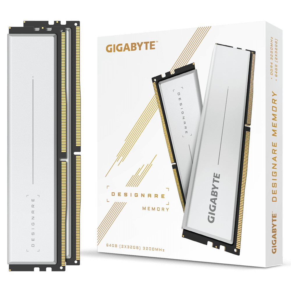
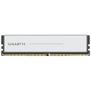
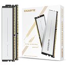
GIGABYTE Rolls Out Designare DDR4-3200 High-Capacity 64GB (2x 32GB) Memory for Creators

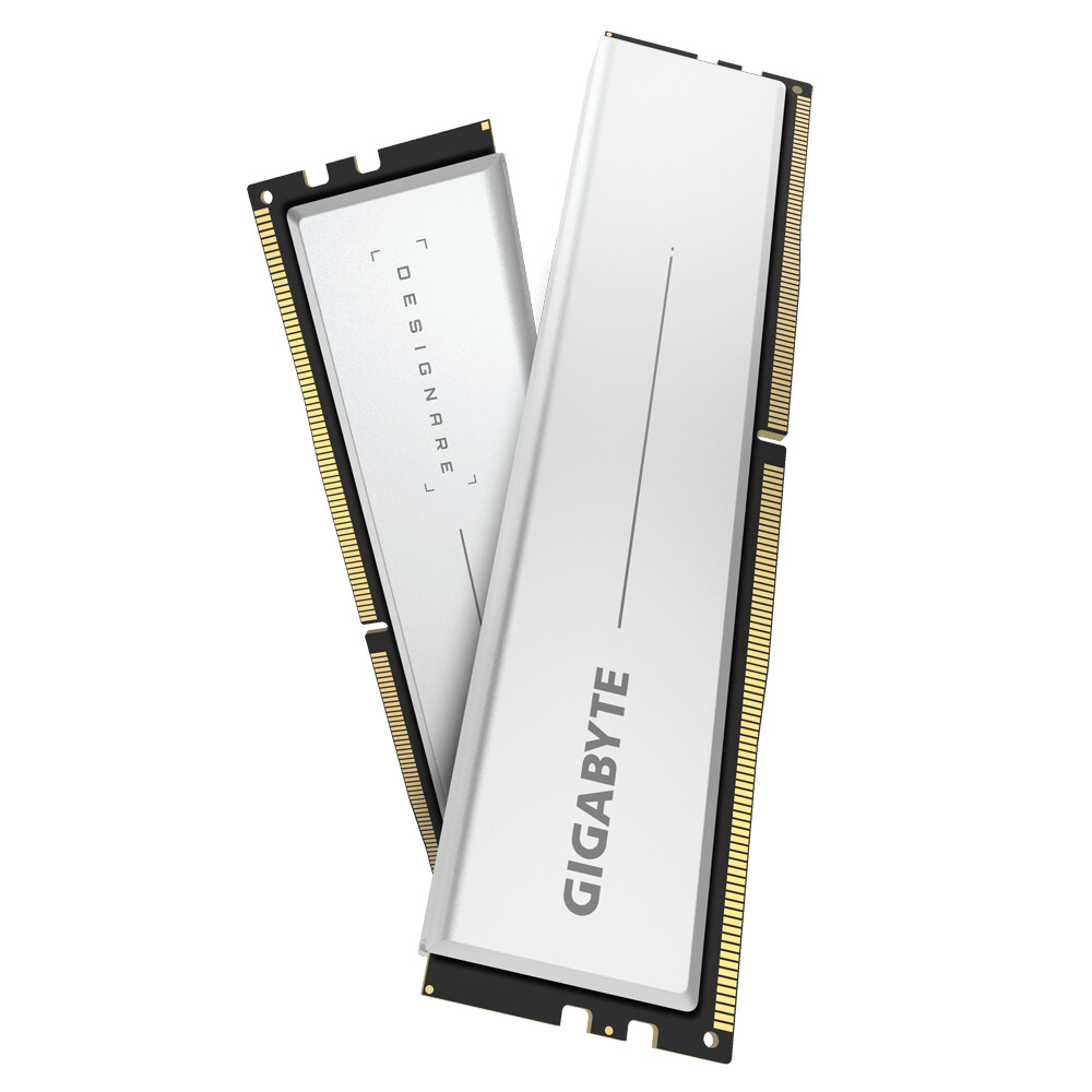
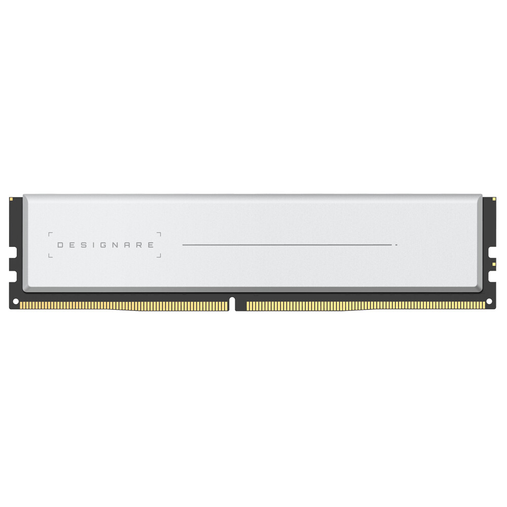
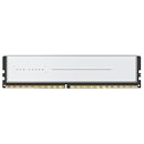
The Designare brand of motherboards by GIGABYTE target content creators, and the company is extending the brand to memory, with the new Designare Memory series. It debuts with a high-capacity 64 GB dual-channel memory kit using two 32 GB modules. The rationale behind these densities is that creators may need them to deal with large data-sets. These are not off-spec "double height" modules, but are common dual-rank modules that stick to JEDEC compatibility spec, and pack XMP profiles that can run them at DDR4-3200 with 16-18-18-38 timings at 1.35 V.

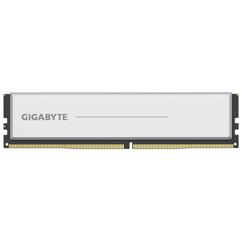
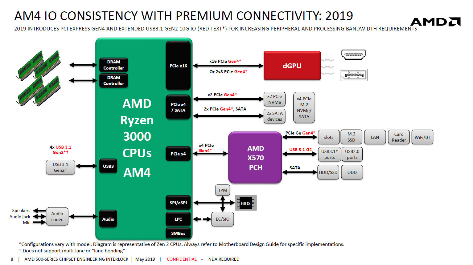
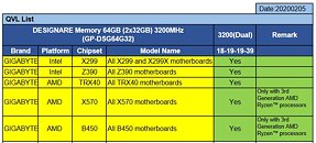
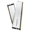
GIGABYTE has tested these modules to work on all of its AMD X570, AMD B450, AMD TRX40, Intel X299, and Intel Z390 motherboards. For X570 and B450, however, the company states that only 3rd generation "Matisse" processors can handle this memory density. In its compatibility testing, GIGABYTE used 18-19-19-39 timings. Physically, the Designare modules have regular 32 mm height, a black PCB, and aluminium heatspreaders. GIGABYTE is backing the modules with lifetime warranty. The company didn't reveal pricing.

DRAM Calculator for Ryzen by 1usmus v1.7.0 Released

DRAM Calculator for Ryzen by 1usmus is the definitive utility to demystify memory overclocking and optimization on AMD Ryzen-powered PCs. It lets you feed in settings you know, and calculates the most optimal related settings (such as latencies), so you get the most from your memory overclock. Version 1.7.0 adds certain memory benchmarks to the utility, including a benchmark for memory bandwidth (reads and writes), and AMD processor inter-core latency tests. The new version also spares you of having to manually input certain current values, by adding the ability to read current memory timings for machines powered by Ryzen 3000-series "Matisse" processors. The new version also adds support for Ryzen Threadripper 3000 "Castle Peak" processor series. Support is also added for SK hynix DJR memory modules. Grab DRAM Calculator for Ryzen from the link below.

DOWNLOAD: DRAM Calculator for Ryzen by 1usmus v1.7.0

AMD CEO To Unveil "Zen 3" Microarchitecture at CES 2020

A prominent Taiwanese newspaper reported that AMD will formally unveil its next-generation "Zen 3" CPU microarchitecture at the 2020 International CES. Company CEO Dr Lisa Su will head an address revealing three key client-segment products under the new 4th generation Ryzen processor family, and the company's 3rd generation EPYC enterprise processor family based on the "Milan" MCM that succeeds "Rome." AMD is keen on developing an HEDT version of "Milan" for the 4th generation Ryzen Threadripper family, codenamed "Genesis Peak."

The bulk of the client-segment will be addressed by two distinct developments, "Vermeer" and "Renoir." The "Vermeer" processor is a client-desktop MCM that succeeds "Matisse," and will implement "Zen 3" chiplets. "Renoir," on the other hand, is expected to be a monolithic APU that combines "Zen 2" CPU cores with an iGPU based on the "Vega" graphics architecture, with updated display- and multimedia-engines from "Navi." The common thread between "Milan," "Genesis Peak," and "Vermeer" is the "Zen 3" chiplet, which AMD will build on the new 7 nm EUV silicon fabrication process at TSMC. AMD stated that "Zen 3" will have IPC increases in line with a new microarchitecture.

New DRAM Calculator for Ryzen v1.6.0.1 Adds Full Ryzen 3000 and X570 Support

Our resident AMD Ryzen memory tuning guru Yuri "1usmus" Bubliy released DRAM Calculator for Ryzen version 1.6.0.1, which comes loaded with support for 3rd generation Ryzen processors based on the "Zen 2" architecture, motherboards based on AMD X570 chipset, and an exhaustive list of new features, and bug-fixes. AMD made major changes to the memory controllers of its Ryzen "Matisse" processors over past generations, including changing the various clock-domains and their interdependence, broader support for overclock across various memory vendors, and more, with the intention of improving memory overclocking. These also mean additional settings to be made in the UEFI BIOS setup programs. DRAM Calculator for Ryzen v1.6.0.1 greatly simplifies that, to help you simply key in the values it calculates based the system configuration it detects or you specify.

DRAM Calculator for Ryzen v1.6.0 also introduces presets for AMD X399 platform and Threadripper processors, helping out the HEDT crowd. Among the key changes are VDDG and FCLK for Zen 2, Vref (CHA / CHB) recommendations; PMU training recommendations that greatly stabilize the overclock; updated presets for Samsung b-die, Hynix CJR and Micron e-die memory modules; support for "Zen 2" processors on older-generations of motherboards (AMD 300-series and 400-series chipsets); improved tWRRD prediction for Dual Rank memory setups; an in-app shortcut to Internet overclocking statistics generation Zen 2; two new settings for MEMBench, the internal stability benchmark; and the overall stability of the program. Grab it from the link below.

DOWNLOAD: DRAM Calculator for Ryzen v1.6.0.1

The change-log follows.

AMD Ryzen 5 3500 a 6-core Processor

AMD is giving final touches to a second wave of 3rd generation Ryzen processor family, which includes the new Ryzen 5 3500 processor, and "Pro" variants of various already-launched SKUs, such as the 3600X, 3700X, and 3900X. These chips were spotted in an import registry of the Eurasian Economic Union. The most interesting bit from this disclosure is the fact that the Ryzen 5 3500 is a 6-core processor with 65 W TDP. For the previous two generations of Ryzen processors, AMD configured its x500 series SKUs, such as the 2500X and 1500X, as 4-core/8-thread processors. It's likely that the 3500 will be a slightly lower-clocked sibling of the Ryzen 5 3600, priced lower, to compete with Intel chips such as the Core i5-9400 or i5-9500. This also raises the possibility of Ryzen 3 "Matisse" processors being 4-core/8-thread chips.

BIOSTAR Formally Enables PCIe Gen 4 on its AMD 400-series Motherboards

BIOSTAR formally (officially) enabled PCI-Express gen 4.0 support for four of its socket AM4 motherboard models based on the AMD X470 and B450 chipsets, through BIOS updates. The updated BIOS lets you use PCI-Express gen 4.0 graphics cards on the topmost PCI-Express x16 slot, and the M.2 NVMe slot that's directly wired to the AM4 SoC. The expansion slots that are wired to the chipset are still restricted to PCIe gen 2.0. You will need a 3rd generation Ryzen "Matisse" processor for PCI-Express gen 4.0. Among the motherboards that receive PCIe gen 4.0 support through BIOS updates are the AB45C-M4S (B450MH), the AB35G-M4S (B45M2), the AX47A-A4T (X470GT8), and the AX47A-I4S (X470GTN). The links lead to the BIOS image files on BIOSTAR website, which you use at your own risk.

Reports of Ryzen 3000 High Idle Voltage Exaggerated, a Case of the "Observer Effect"

With AMD's 3rd generation Ryzen processors finally falling into the hands of PC enthusiasts, many early-adopters are taking to tech communities such as ours, to share their experiences with others. A trend appears to be emerging of users reporting higher-than-usual voltages for these processors when idling. AMD investigated this phenomenon, and declared this to be a non-issue. Apparently, most modern CPU monitoring utilities cause what is known as "the observer effect:" the process of measuring the processor's load itself causes load on the processor.

In case of the Ryzen "Matisse" processors, monitoring software appear to be polling each processor core for load by sending it instruction at a high rate of speed - sending them a workload of 20 ms every 200 ms. This causes the processor's embedded firmware to think that the cores are being subjected to workload, and it responds by increasing the clock-speeds, and proportionately voltages of all CPU cores. Monitoring software poll each CPU core, and so core voltages are raised across the chip.

Bitspower Unveils the Touchaqua CPU Block Summit MS For AM4 Processors

Bitspower today unveiled the Touchaqua series Summit MS for AMD socket AM4. The block is designed for full coverage of the AMD socket AM4 processor IHS, and can uniformly cool even the latest "Matisse" MCMs since its micro-fin lattice is spread across a wider area than most other socket AM4 blocks. The primary material is copper, with a central portion that has a mirror-finish; while the top is made of acrylic with an embedded addressable-RGB strip that takes in 3-pin aRGB input. The block measures 111 mm x 73 mm x 20.3 mm (LxWxH), and takes in standard G 1/4" fittings. The block is now available for pre-order from Bitspower website.

AMD Ryzen 9 3950X Cinebench R15 Performance Spied

Market availability of the 16-core Ryzen 9 3950X may be far away, given its September 2019 launch, but engineering samples (ESes) of the chip seem to be already in circulation. "uzzi38" on Twitter posted this spy-shot of a 3950X ES making short work of Cinebench R15. CPU-Z recognizes the chip by its codename "Matisse," and puts out the correct CPU core and thread count, but doesn't give a name-string. It also recognizes the MSI MEG X570 GODLIKE motherboard this test is run on.

The purported Ryzen 9 3950X ES, overclocked to 5.42 GHz, scores a gargantuan 5,501 points in the multi-threaded benchmark. To put this number into perspective, at stock frequencies, a Ryzen Threadripper 2950X (same core-count, double the memory bus width), scores 3,645 points. The 3950X benefits from not just its massive overclock that's over 1 GHz higher than the stock TR-2950X, but also higher IPC, and a more consolidated memory interface. This feat goes to show that AMD's upcoming Ryzen chips love to overclock, and deliver a significantly higher single-thread performance over the previous generation.

Intel "Ice Lake" IPC Best-Case a Massive 40% Uplift Over "Skylake," 18% on Average

Intel late-May made its first major disclosure of the per-core CPU performance gains achieved with its "Ice Lake" processor that packs "Sunny Cove" CPU cores. Averaged across a spectrum of benchmarks, Intel claims a best-case scenario IPC (instructions per clock) uplift of a massive 40 percent over "Skylake," and a mean uplift of 18 percent. The worst-case scenario sees its performance negligibly below that of "Skylake." Intel's IPC figures are derived entirely across synthetic benchmarks, which include SPEC 2016, SPEC 2017, SYSMark 2014 SE, WebXprt, and CineBench R15. The comparison to "Skylake" is relevant because Intel has been using essentially the same CPU core in the succeeding three generations that include "Kaby Lake" and "Coffee Lake."

A Chinese tech-forum member with access to an "Ice Lake" 6-core/12-thread sample put the chip through the CPU-Z internal benchmark (test module version 17.01). At a clock-speed of 3.60 GHz, the "Ice Lake" chip allegedly achieved a single-core score of 635 points. To put this number into perspective, a Ryzen 7 3800X "Matisse" supposedly needs to run at 4.70 GHz to match this score, and a Core i7-7700K "Kaby Lake" needs to run at 5.20 GHz. Desktop "Ice Lake" processors are unlikely to launch in 2019. The first "Ice Lake" processors are 4-core/8-thread chips designed for ultraportable notebook platforms, which come out in Q4-2019, and desktop "Ice Lake" parts are expected only in 2020.

AMD Ryzen 3000 "Matisse" I/O Controller Die 12nm, Not 14nm

AMD Ryzen 3000 "Matisse" processors are multi-chip modules of two kinds of dies - one or two 7 nm 8-core "Zen 2" CPU chiplets, and an I/O controller die that packs the processor's dual-channel DDR4 memory controller, PCI-Express gen 4.0 root-complex, and an integrated southbridge that puts out some SoC I/O, such as two SATA 6 Gbps ports, four USB 3.1 Gen 2 ports, LPCIO (ISA), and SPI (for the UEFI BIOS ROM chip). It was earlier reported that while the Zen 2 CPU core chiplets are built on 7 nm process, the I/O controller is 14 nm. We have confirmation now that the I/O controller die is built on the more advanced 12 nm process, likely GlobalFoundries 12LP. This is the same process on which AMD builds its "Pinnacle Ridge" and "Polaris 30" chips. The 7 nm "Zen 2" CPU chiplets are made at TSMC.

AMD also provided a fascinating technical insight to the making of the "Matisse" MCM, particularly getting three highly complex dies under the IHS of a mainstream-desktop processor package, and perfectly aligning the three for pin-compatibility with older generations of Ryzen AM4 processors that use monolithic dies, such as "Pinnacle Ridge" and "Raven Ridge." AMD innovated new copper-pillar 50µ bumps for the 8-core CPU chiplets, while leaving the I/O controller die with normal 75µ solder bumps. Unlike with its GPUs that need high-density wiring between the GPU die and HBM stacks, AMD could make do without a silicon interposer or TSVs (through-silicon-vias) to connect the three dies on "Matisse." The fiberglass substrate is now "fattened" up to 12 layers, to facilitate the inter-die wiring, as well as making sure every connection reaches the correct pin on the µPGA.

AMD X570 Puts Out Up To Twelve SATA 6G Ports and Sixteen PCIe Gen 4 Lanes

AMD X570 is the company's first in-house design desktop motherboard chipset for the AM4 platform. The company sourced earlier generations of chipset from ASMedia. A chipset in context of the AM4 platform only serves to expand I/O connectivity, since an AM4 processor is a full-fledged SoC, with an integrated southbridge that puts out SATA and USB ports directly from the CPU socket, in addition to LPCIO (ISA), HD audio bus, and SPI to interface with the firmware ROM chip. The X470 "Promontory Low Power" chipset runs really cool, with a maximum TDP of 5 Watts, and the ability to lower power to get its TDP down to 3W. The X570, on the other hand, has a TDP of "at least 15 Watts." A majority of the X570 motherboards we've seen at Computex 2019 had active fan-heatsinks over the chipset. We may now have a possible explanation for this - there are just too many things on the chipset.

According to AMD, the X570 chipset by itself can be made to put out a staggering twelve SATA 6 Gbps ports (not counting the two ports put out by the AM4 SoC). A possible rationale behind this may have been to enable motherboard designers to equip every M.2 slot on the motherboard with SATA wiring in addition to PCIe, without needing switches that reroute SATA connection from one of the physical ports. It's also possible that AMD encouraged motherboard designers to not wire out SATA ports from the AM4 SoC as physical ports to save costs on switches, and dedicate one of them to the M.2 slot wired to the SoC. With the two SATA ports from the SoC out of the equation, and every other M.2 slot getting a direct SATA connection from the chipset, motherboard designers can wire out the remaining SATA ports as physical ports, without spending money on switches, or worrying about customer complaints on one of their drives not working due to automatic switching. This is an extreme solution to a rather simple problem.

AMD Readies Ryzen 9 3950X 16-core Processor to Awestrike Crowds at E3

When AMD launched its Ryzen 9 3900X 12-core/24-thread processor at its Computex 2019 keynote, our readers commented on the notable absence of a 16-core SKU, given that a "Matisse" multi-chip module with two 8-core "Zen 2" chiplets adds up to that core-count. Some readers noted this could be a case of AMD holding back its top performing part in the absence of competition in the segment from Intel. It turns out, the company was saving this part up for an E3 2019 unveiling.

The Ryzen 9 3950X maxes out "Matisse" MCM with 16 cores, 32 threads via SMT, a staggering 64 MB of L3 cache (72 MB including the 8 MB of total L2 cache), and a stunning 105-Watt TDP figure that's unchanged from the company's TDP for the 3900X. The Ryzen 9 3950X is clocked at 3.50 GHz, with a maximum boost frequency of 4.70 GHz. The company is yet to reveal its price, but given that the $499 price-tag has already been taken by the 3900X, one could expect an even higher price. It remains to be seen if the 3950X will launch alongside the rest of the series on 7/7.

Intel Challenges AMD to Beat it in "Real World Gaming"

AMD is on the verge of launching its 3rd generation Ryzen "Matisse" processors that are widely expected to take the performance crown from Intel. At its Computex 2019 reveal, AMD CEO Dr Lisa Su claimed that these processors beat the competition in all areas, including gaming. Motherboard manufacturers threw their weight behind AMD by pulling out their most premium brands for the AMD "Valhalla" desktop platform that consists of these processors, mated with an AMD X570 chipset motherboard. Ahead of its E3 2019 keynote Monday afternoon, Intel has come out with a challenge. Chipzilla dares AMD to beat it in "real-world gaming."

At its "gaming performance for the real world" address in Los Angeles Jon Carvill, VP of marketing, challenged AMD to beat it in real world gaming with its upcoming processors. "So you're going to hear a lot about gaming CPUs this week," he began. "They may or may not come from certain three letter acronyms. That said, here's what I want to challenge you. I want to challenge you to challenge them. If they want this crown come beat us in in real world gaming, real world gaming should be the defining criteria that we use to assess the world's best gaming CPU. I challenge you to challenge anyone that wants to compete for this crown to come meet us in real world gaming. That's the measure that we're going to stand by."

ADATA Shows Off a JEDEC-compliant 32GB Dual-rank DIMM That Isn't "Double Capacity"

Last year, with the introduction of the Intel Z390 chipset, there was a spate of so-called "double capacity DIMMs" or DC DIMMs, tall memory modules with two rows of DRAM chips, which added up to 32 GB per DIMM. You needed a Z390 platform and a 9th generation Core processor that supported up to 128 GB of memory, to use these things. With the introduction of 16 Gb DDR4 DRAM chips by both Micron and Samsung, JEDEC-compliant 32 GB unbuffered DIMMs of standard height are finally possible, and ADATA put together the first of these, shown off at Computex 2019.

The AD4U2666732GX16 is a 32-gigabyte dual-rank unbuffered DIMM made using 16 Gb chips supplied by Micron Technology. The modules tick at JEDEC-standard DDR4-2666 speeds, at a module voltage of 1.2 Volts. ADATA didn't disclose timings. The 16 Gb DRAM chips are made by Micron in an advanced (3rd generation) 10 nm-class silicon fabrication process to achieve the desired transistor-density. 32 GB DIMMs are expected to hit critical-mass in 2H-2019/2020, with the advent of AMD's 3rd generation Ryzen "Matisse," and Intel's "Ice Lake-S" desktop processors. Memory manufacturers are also expected to put out speedy and highly-compatible single-rank 16-gigabyte DIMMs using 16 Gb chips, which could finally make 32 GB dual-channel the mainstream memory configuration, moving up from half a decade of 2x 8 GB.

AMD 300-series and 400-series Motherboards to Lack PCIe Gen 4 with Ryzen 3000

This shouldn't really need to be spelled out, but AMD clarified that you can't have PCI-Express gen 4.0 running an upcoming Ryzen 3000 "Matisse" processor on older socket AM4 motherboards based on AMD 300-series and 400-series chipsets, and that the processor's PCIe root-complex will run at PCI-Express gen 3.0 speeds. AMD's official reason for this is that the older motherboards can't guarantee reliable signaling needed for PCI-Express gen 4.0 and hence the company decided to blanket-disable PCIe gen 4.0 for the older platforms. This statement was put out by Robert Hallock, senior technical marketing head for CPUs and APUs, on Reddit.

Unofficially, though, we believe there are technological barriers standing in the way of PCI-Express gen 4.0 on the older motherboards, the least of which are the lack of external PCIe gen 4.0-certified re-driver/equalizer components, and lane-switching on boards that split one x16 PEG link to two x8 links. There may be other less technical issues such as PCI-SIG certification for the older platforms. Intel faced a similar challenge with its 3rd generation Core "Ivy Bridge" processors, which introduced PCI-Express gen 3.0 to the mainstream desktop platform, and were backwards-compatible with Intel 6-series chipset (eg: Z68 Express). The older 6-series motherboards could only put out PCIe gen 2.0 with the newer processors.

AMD Confirms Ryzen 3000 "Matisse" Features Soldered IHS

AMD senior technical marketing manager Robert Hallock, responding to a specific question on Twitter, confirmed that the 3rd generation Ryzen processors do feature soldered integrated heatspreaders (IHS). Soldering as an interface material is preferred as it offers better heat transfer between the processor die and the IHS, as opposed to using a fluid TIM such as pastes. "Matisse" will be one of the rare few examples of a multi-chip module with a soldered IHS. The package has two kinds of dies, one or two 7 nm "Zen 2" 8-core CPU chiplets, and one 14 nm I/O Controller die.

The most similar example of such a processor would be Intel's "Clarkdale" (pictured below), which has its CPU cores sitting on a 32 nm die, while the I/O, including memory controller and iGPU, are on a separate 45 nm die. On-package QPI connects the two. Interestingly, Intel used two different sub-IHS interface materials for "Clarkdale." While the CPU die was soldered, a fluid TIM was used for the I/O controller die. It would hence be very interesting to see if AMD solders both kinds of dies under the "Matisse" IHS, or just the CPU chiplets. Going by Hallock's strong affirmative "Like a boss," we lean toward the possibility of all dies being soldered.
Image Credit: TheLAWNOOB (OCN Forums)

ASUS Teases Collage of Upcoming AMD X570 Motherboards

With AMD expected to launch its 3rd generation Ryzen processor family at the 2019 Computex, the show is expected to have unveilings of several compatible motherboards based on the new AMD X570 chipset. ASUS posted a collage picture that teases its upcoming X570 lineup. This appears to include boards from pretty much all of ASUS's brands, including the high-end ROG Crosshair, the upper mainstream ROG Strix, the mainstream TUF Gaming, and the sober Prime series. From this, the ROG Strix board appears to be the first one we've come across that doesn't use a fan-heatsink to cool the 15W TDP X570 chipset. The Ryzen 3000 "Matisse" processor and X570 chipset make up AMD's "Valhalla" desktop platform.

FinalWire Releases AIDA64 v6.00

FinalWire Ltd. today announced the immediate availability of AIDA64 Extreme 6.00 software, a streamlined diagnostic and benchmarking tool for home users; the immediate availability of AIDA64 Engineer 6.00 software, a professional diagnostic and benchmarking solution for corporate IT technicians and engineers; the immediate availability of AIDA64 Business 6.00 software, an essential network management solution for small and medium scale enterprises; and the immediate availability of AIDA64 Network Audit 6.00 software, a dedicated network audit toolset to collect and manage corporate network inventories.

The latest AIDA64 update introduces SHA3-512 cryptographic hash benchmark and AVX2 optimized benchmarks for the upcoming AMD Zen 2 "Matisse" processors, adds monitoring of sensor values on BeadaPanel LCD displays, and supports the latest AMD and Intel CPU platforms as well as the new graphics and GPGPU computing technologies by both AMD and NVIDIA.
DOWNLOAD: FinalWire AIDA64 v6.00

AMD X570 Unofficial Platform Diagram Revealed, Chipset Puts out PCIe Gen 4

AMD X570 is the company's first in-house design socket AM4 motherboard chipset, with the X370 and X470 chipsets being originally designed by ASMedia. With the X570, AMD hopes to leverage new PCI-Express gen 4.0 connectivity of its Ryzen 3000 Zen2 "Matisse" processors. The desktop platform that combines a Ryzen 3000 series processor with X570 chipset is codenamed "Valhalla." A rough platform diagram like what you'd find in motherboard manuals surfaced on ChipHell, confirming several features. To maintain pin-compatibility with older generations of Ryzen processors, Ryzen 3000 has the same exact connectivity from the SoC except two key differences.

On the AM4 "Valhalla" platform, the SoC puts out a total of 28 PCI-Express gen 4.0 lanes. 16 of these are allocated to PEG (PCI-Express graphics), configurable through external switches and redrivers either as single x16, or two x8 slots. Besides 16 PEG lanes, 4 lanes are allocated to one M.2 NVMe slot. The remaining 4 lanes serve as the chipset bus. With X570 being rumored to support gen 4.0 at least upstream, the chipset bus bandwidth is expected to double to 64 Gbps. Since it's an SoC, the socket is also wired to LPCIO (SuperIO controller). The processor's integrated southbridge puts out two SATA 6 Gbps ports, one of which is switchable to the first M.2 slot; and four 5 Gbps USB 3.x ports. It also has an "Azalia" HD audio bus, so the motherboard's audio solution is directly wired to the SoC. Things get very interesting with the connectivity put out by the X570 chipset.
Update May 21st: There is also information on the X570 chipset's TDP.
Update May 23rd: HKEPC posted what looks like an official AMD slide with a nicer-looking platform map. It confirms that AMD is going full-tilt with PCIe gen 4, both as chipset bus, and as downstream PCIe connectivity.

AMD Ryzen 9 3000 is a 16-core Socket AM4 Beast

AMD is giving finishing touches to its 3rd generation Ryzen socket AM4 processor family which is slated for a Computex 2019 unveiling, followed by a possible E3 market availability. Based on the "Matisse" multi-chip module that combines up to two 8-core "Zen 2" chiplets with a 14 nm I/O controller die, these processors see a 50-100 percent increase in core-counts over the current generation. The Ryzen 5 series now includes 8-core/16-thread parts, the Ryzen 7 series chips are 12-core/24-thread, while the newly created Ryzen 9 series (designed to rival Intel Core i9 LGA115x), will include 16-core/32-thread chips.

Thai PC enthusiast TUM_APISAK confirmed the existence of the Ryzen 9 series having landed himself with an engineering sample of the 16-core/32-thread chip that ticks at 3.30 GHz with 4.30 GHz Precision Boost frequency. The infamous Adored TV leaks that drew the skeleton of AMD's 3rd generation Ryzen roadmap, referenced two desktop Ryzen 9 parts, the Ryzen 9 3800X and Ryzen 9 3850X. The 3800X is supposed to be clocked at 3.90 GHz with 4.70 GHz boost, with a TDP rating of 125W, while the 3850X tops the charts at 4.30 GHz base and a staggering 5.10 GHz boost. The rated TDP has shot up to 135W. We can now imagine why some motherboard vendors are selective with BIOS updates on some of their lower-end boards. AMD is probably maximizing the clock-speed headroom of these chips out of the box, to preempt Intel's "Comet Lake" 10-core/20-thread processor.

Intel 10nm Ice Lake to Quantitatively Debut Within 2019

Intel put out interesting details about its upcoming 10 nanometer "Ice Lake" CPU microarchitecture rollout in its recent quarterly financial results call. The company has started qualification of its 10 nm "Ice Lake" processors. This involves sending engineering samples to OEMs, system integrators and other relevant industry partners, and getting the chips approved for their future product designs. The first implementation of "Ice Lake" will not be a desktop processor, but rather a low-power mobile SoC designed for ultraportables, codenamed "Ice Lake-U." This SoC packs a 4-core/8-thread CPU based on the "Sunny Cove" core design, and Gen11 GT2 integrated graphics with 64 execution units and nearly 1 TFLOP/s compute power. This SoC will also support WiFi 6 and LPDDR4X memory.

Intel CEO Bob Swan also remarked that the company has doubled its 10 nm yield expectations. "On the [10 nm] process technology front, our teams executed well in Q1 and our velocity is increasing," he said, adding "We remain on track to have volume client systems on shelves for the holiday selling season. And over the past four months, the organization drove a nearly 2X improvement in the rate at which 10nm products move through our factories." Intel is prioritizing enterprise over desktop, as "Ice Lake-U" will be followed by "Ice Lake-SP" Xeon rollout in 2020. There was no mention of desktop implementations such as "Ice Lake-S." Intel is rumored to be preparing a stopgap microarchitecture for the desktop platform to compete with AMD "Matisse" Zen 2 AM4 processors, codenamed "Comet Lake." This is essentially a Skylake 10-core die fabbed on existing 14 nm++ node. AMD in its CES keynote announced an achievement of per-core performance parity with Intel, so it could be interesting to see how Intel hopes 10 "Skylake" cores match up to 12-16 "Zen 2" cores.

AMD Ryzen 3 3200G Pictured and De-lidded

AMD Ryzen 3 3200G is an upcoming processor featuring integrated graphics, forming the tail-end of the company's 3rd generation Ryzen desktop processor family. A Chinese PC enthusiast with access to an early sample pictured and de-lidded the processor. We know from older posts that while the "Matisse" MCM will form the bulk of AMD's 3rd gen Ryzen lineup, with core counts ranging all the way from 6 to 12, and possibly 16 later, the APU lineup is rumored to be based on older "Zen+" architecture.

The Ryzen 3 3200G and possibly the Ryzen 5 3400G, will be based on a derivative of the "Raven Ridge" silicon built on the 12 nm process at GlobalFoundries, and comes with a handful innovations AMD introduced with "Pinnacle Ridge," such as an improved Precision Boost algorithm and faster on-die caches. The 12 nm shrink also allows AMD to dial up CPU and iGPU engine clock speeds, and improve DDR4 memory support to work with higher DRAM clock speeds. AMD has used thermal paste as the sub-IHS interface material instead of solder for its "Raven Ridge" chips, and the story repeats with the 3200G.

MSI Betrays AMD's Socket AM4 Longevity Promise: No Zen2 for 300-series?

Greedy motherboard vendors such as MSI want you to buy a new motherboard every two generations of processor for no sound reason at all. MSI is reportedly blocking support for 3rd generation Ryzen "Matisse" processors on its AMD 300-series chipset motherboards, including those based on high-end AMD X370 and OC-capable B350 chipsets. This would also put those who own $300 motherboards such as the X370 XPower out of luck. To recap, AMD announced on numerous occasions that it doesn't want to be a greedy clique like its competitor, by forcing motherboard upgrades and promised that socket AM4 motherboards will be backwards and forwards compatible with at least four generations of Ryzen processors, running all the way up to 2020.

This normally should mean that any 300-series motherboard must support 4th generation Ryzen processors with a simple BIOS update. Most 300-series motherboards, including from MSI, even ship with USB BIOS Flashback feature to help with forwards compatibility. Unfortunately, motherboard companies such as MSI care more about their bottom-lines than the consumer. In a support e-mail to an X370 XPower Titanium owner, MSI confirmed that it will not extend Zen 2 support to AMD 300-series. Other motherboard vendors could follow MSI's suit as a representative of another motherboard vendor, on condition of anonymity, told TechPowerUp that "Zen 2" processors have steeper electrical requirements that 300-series motherboards don't meet. This is an excuse similar to the one Intel gave for the planned obsolescence of its 100-series and 200-series chipsets, even as it was repeatedly proven that those motherboards can run and overclock 9th generation processors with custom firmware just fine. Would MSI care to explain whether a B450M PRO-M2 has a stronger VRM than an X370 XPower Titanium to warrant "Zen 2" support? Will all "Zen 2" processor SKUs have steep electrical requirements? Will there not be any SKUs with double-digit-Watt TDP ratings?

Update (16/04): MSI posted a clarification on this issue.

AMD "Castle Peak," "Rome," and "Matisse" Referenced in Latest AIDA64 Changelog

FinalWire over the past week posted the latest public beta of AIDA64, which adds support for the three key processor product lines based on AMD's "Zen 2" microarchitecture. The "Matisse" multi-chip module, which received extensive coverage over the past few weeks, will be AMD's main derivative of "Zen 2," designed for the client-segment socket AM4 platform, with up to 16 CPU cores, and the initial flagship product featuring 12 cores. "Rome" is AMD's all-important enterprise-segment MCM for the SP3 platform, with up to 64 CPU cores spread across eight 8-core chiplets interfacing a centralized I/O controller die with a monolithic 8-channel memory controller. It so happens that AMD also wants to update its Ryzen Threadripper line of high-end desktop processors, with "Castle Peak."

"Castle Peak" is codename for 3rd generation Ryzen Threadripper and a client-segment derivative of the "Rome" MCM with a reconfigured I/O controller die that has a monolithic 4-channel DDR4 memory interface, and an unspecified number of CPU cores north of 24. This is for backwards compatibility with the existing AMD X399 motherboards. AMD configures core-count by physically changing the number of 8-core chiplets on the MCM, in addition to disabling cores in groups of 2 within the chiplet. The company could scale core counts looking at its competitive environment. The monolithic quad-channel memory interface could significantly improve the chip's memory performance compared to current-generation Threadrippers, particularly the Threadripper WX series chips in which half the CPU cores are memory bandwidth-starved. The AIDA64 update also improves detection of existing Ryzen/EPYC processors with the K17.3 and K17.5 integrated northbridges.

DOWNLOAD: FinalWire AIDA64 Extreme 5.99.4983 beta
Return to Keyword Browsing
Apr 18th, 2024 18:03 EDT change timezone

New Forum Posts

Popular Reviews

Controversial News Posts