News Posts matching #Photonics

Return to Keyword Browsing

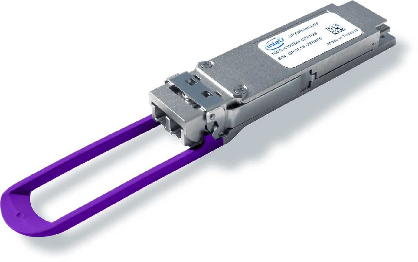
Jabil to Take Over Intel Silicon Photonics Business

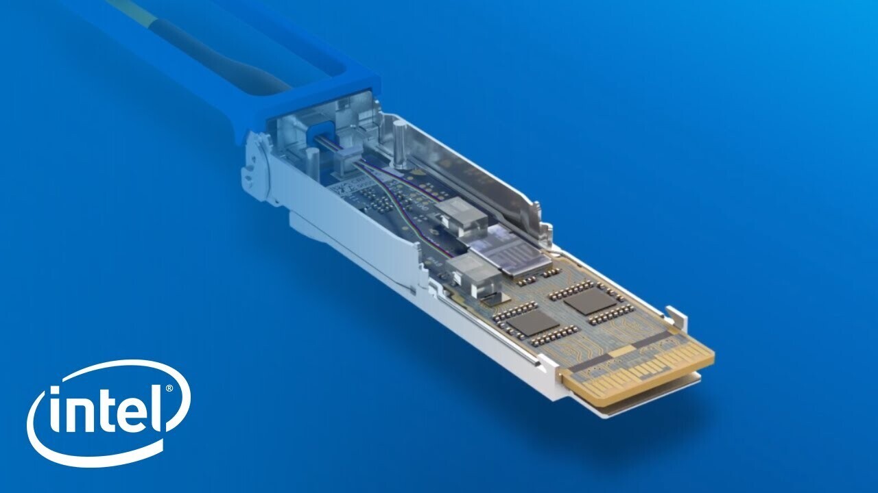
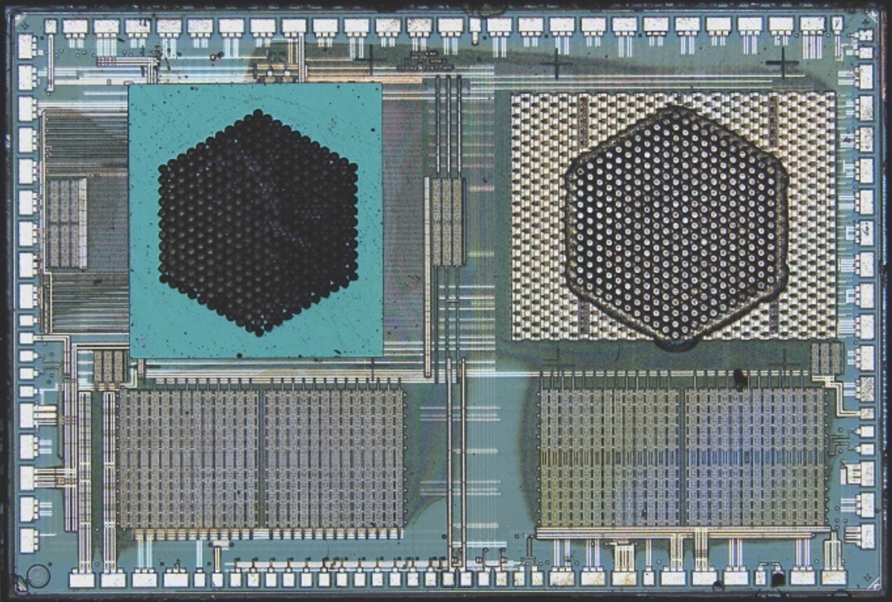
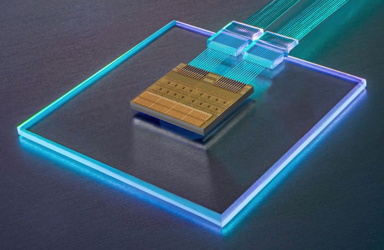
Jabil Inc., a global leader in design, manufacturing, and supply chain solutions, today announced it will take over the manufacture and sale of Intel's current Silicon Photonics-based pluggable optical transceiver ("module") product lines and the development of future generations of such modules.

"This deal better positions Jabil to cater to the needs of our valued customers in the data center industry, including hyperscale, next-wave clouds, and AI cloud data centers. These complex environments present unique challenges, and we are committed to tackling them head-on and delivering innovative solutions to support the evolving demands of the data center ecosystem," stated Matt Crowley, Senior Vice President of Cloud and Enterprise Infrastructure at Jabil. "This deal enables Jabil to expand its presence in the data center value chain."

Avicena Demonstrates First microLED Based Transceiver IC in 16 nm finFET CMOS for Chip-to-Chip Communications

Avicena, a privately held company headquartered in Sunnyvale, CA, is demonstrating its LightBundle multi-Tbps chip-to-chip interconnect technology at the European Conference for Optical Communications (ECOC) 2023 in Glasgow, Scotland (https://www.ecocexhibition.com/). Avicena's microLED-based LightBundle architecture breaks new ground by unlocking the performance of processors, memory and sensors, removing key bandwidth and proximity constraints while simultaneously offering class leading energy efficiency.

"As generative AI continues to evolve, the role of high bandwidth-density, low-power and low latency interconnects between xPUs and HBM modules cannot be overstated", says Chris Pfistner, VP Sales & Marketing of Avicena. "Avicena's innovative LightBundle interconnects have the potential to fundamentally change the way processors connect to each other and to memory because their inherent parallelism is well-matched to the internal wide and slow bus architecture within ICs. With a roadmap to multi-terabit per second capacity and sub-pJ/bit efficiency these interconnects are poised to enable the next era of AI innovation, paving the way for even more capable models and a wide range of AI applications that will shape the future."

TSMC, Broadcom & NVIDIA Alliance Reportedly Set to Advance Silicon Photonics R&D

Taiwan's Economic Daily reckons that a freshly formed partnership between TSMC, Broadcom, and NVIDIA will result in the development of cutting-edge silicon photonics. The likes of IBM, Intel and various academic institutes are already deep into their own research and development processes, but the alleged new alliance is said to focus on advancing AI computer hardware. The report cites a significant allocation of—roughly 200—TSMC staffers onto R&D involving the integration of silicon photonic technologies into high performance computing (HPC) solutions. They are very likely hoping that the usage of optical interconnects (on a silicon medium) will result in greater data transfer rates between and within microchips. Other benefits include longer transmission distances and a lower consumption of power.

TSMC vice president Yu Zhenhua has placed emphasis on innovation, in a similar fashion to his boss, within the development process (industry-wide): "If we can provide a good silicon photonics integrated system, we can solve the two key issues of energy efficiency and AI computing power. This will be a new one...Paradigm shift. We may be at the beginning of a new era." The firm is facing unprecedented demand from its clients—it hopes to further expand its advanced chip packaging capacity to address these issues by late 2024. A shift away from the limitations of "conventional electric" data transmissions could bring next generation AI compute GPUs onto the market by 2025.

Ayar Labs Demonstrates Industry's First 4-Tbps Optical Solution, Paving Way for Next-Generation AI and Data Center Designs

Ayar Labs, a leader in the use of silicon photonics for chip-to-chip optical connectivity, today announced public demonstration of the industry's first 4 terabit-per-second (Tbps) bidirectional Wavelength Division Multiplexing (WDM) optical solution at the upcoming Optical Fiber Communication Conference (OFC) in San Diego on March 5-9, 2023. The company achieves this latest milestone as it works with leading high-volume manufacturing and supply partners including GlobalFoundries, Lumentum, Macom, Sivers Photonics and others to deliver the optical interconnects needed for data-intensive applications. Separately, the company was featured in an announcement with partner Quantifi Photonics on a CW-WDM-compliant test platform for its SuperNova light source, also at OFC.

In-package optical I/O uniquely changes the power and performance trajectories of system design by enabling compute, memory and network silicon to communicate with a fraction of the power and dramatically improved performance, latency and reach versus existing electrical I/O solutions. Delivered in a compact, co-packaged CMOS chiplet, optical I/O becomes foundational to next-generation AI, disaggregated data centers, dense 6G telecommunications systems, phased array sensory systems and more.

POINTek Shows Off Optical Fiber Array Product Families for Silicon Photonics Integrated Chips

POINTek, Inc., a global leader and provider of high performance athermal AWGs, announced launching of new Application- Specific Optical Fiber Array Products, Silicon Photonics (SiPh) Fiber Arrays, which is capable of supporting the back-end packaging for Silicon Photonics Integrated Circuits (PIC). This new Silicon Photonics Fiber Arrays have the excellent characteristics of a fine fiber-end mirror-surface quality and an accurate fiber protrusion length uniformity to match with the prefabricated V-grooves on a Silicon PIC chip. The required fiber protrusion length is typically 5 mm with ≤ ±2 um length uniformity in an array. Both Single Mode (SM) Fiber Arrays and Polarization Maintaining (PM) Fiber Arrays are available with or without 12-channel MT ferrule termination.

"This new SiPh Fiber Array is designed to passively align the multiple optical fibers into the wafer-fabricated V-grooves on the Silicon PIC chip without the expensive and complicated active alignment equipment, and furthermore, the passive alignment of the Array can be accomplished without monitoring the optical power," according to Dr. Donald Yu, CMO of POINTek, operating from Los Angeles, California. Yu explains that the optical fiber array is a key component to efficiently assemble the PIC devices for coupling the multiple fibers into the multiple I/O waveguides on a PIC chip. In the conventional optical active alignment assembly process, the expensive automatic precision alignment equipment should be utilized while monitoring the optical power in the packaging process, and it often takes the long processing time. "However, for this new SiPh Fiber Array, the fibers can be precisely placed in the Silicon PIC's V-grooves with the minimal operation costs. Therefore, the passive alignment of Silicon PIC could result in the very affordable SiPh device price in the market," Yu adds.

Folio Photonics Announces Breakthrough Multi-Layer Optical Disc Storage: 10 TB for $50

Folio Photonics, a leading pioneer of immutable active archive, today announced that it has achieved a significant breakthrough in multi-layer optical storage disc technology that will enable an unprecedented level of cost, security and sustainability advantage. Leveraging patented advancements in materials science, Folio Photonics has developed the first economically viable, enterprise-scale optical storage discs with dynamic multi-layer write/read capabilities, which will enable the development of radically low-cost/high-capacity disc storage.

"Folio Photonics is on a path to engendering far greater data densities than was thought possible several years ago," said John Monroe, lead analyst at Furthur Market Research and former VP analyst in the data center infrastructure group at Gartner. "Using next-generation materials, patented polymer extrusion, and film-based disc construction processes (distinct from mere optical layering), in concert with customized optical pickup units (OPUs), Folio Photonics appears poised to deliver a new optical technology that enables eight or 16 film layers per side per disc, as opposed to only three optical layers per side per disc for archival discs today, with a roadmap to add additional layers over time."

Intel Labs Announces Integrated Photonics Research Advancement

Intel Labs announces a significant advancement in its integrated photonics research - the next frontier in increasing communication bandwidth between compute silicon in data centers and across networks. The latest research features industry-leading advancements in multiwavelength integrated optics, including the demonstration of an eight-wavelength distributed feedback (DFB) laser array that is fully integrated on a silicon wafer and delivers excellent output power uniformity of +/- 0.25 decibel (dB) and wavelength spacing uniformity of ±6.5% that exceed industry specifications.

"This new research demonstrates that it's possible to achieve well-matched output power with uniform and densely spaced wavelengths. Most importantly, this can be done using existing manufacturing and process controls in Intel's fabs, thereby ensuring a clear path to volume production of the next-generation co-packaged optics and optical compute interconnect at scale." -Haisheng Rong, senior principal engineer at Intel Labs

Canada is the Next Nation That is Getting Ready to Invest in the Semiconductor Industry

The Canadian government is getting ready to invest C$240 million (about US$187 million) into what the country calls the Semiconductor Challenge Callout. C$90 million of that will go towards the Canadian Photonics Fabrication Centre (CPFC), which is as the name implies, a facility that engineers and manufactures a range of photonics products, mostly on the prototyping level. The remaining C$150 million is up for grabs through the Strategic Innovation Fund, which is a government fund set up to help Canadian companies grow.

François-Philippe Champagne, the Canadian Minister of Innovation, Science and Industry is quoted as saying "By investing in Canada's semiconductor industry, we are making a firm commitment to businesses looking to invest in Canada. Whether it's high-value or large-scale manufacturing, we want to see Canada be home to the world's leading semiconductor manufacturers.". Exactly which companies will be asking for a share of the money is currently up in the air, but according to The Register, the Canadian government is looking for a wide range of potential semiconductor related businesses. Some examples are 2.5D and 3D chip packaging, MEMS sensor manufacturing and so on. None of this is compared to what the US, EU, Taiwan, Korea and the PRC are currently working on, but it could very well end up being supplemental to much of what's going on in the US semiconductor market right now.

Intel Launches Integrated Photonics Research Center

Intel Labs recently opened the Intel Research Center for Integrated Photonics for Data Center Interconnects. The center's mission is to accelerate optical input/output (I/O) technology innovation in performance scaling and integration with a specific focus on photonics technology and devices, CMOS circuits and link architecture, and package integration and fiber coupling.

"At Intel Labs, we're strong believers that no one organization can successfully turn all the requisite innovations into research reality. By collaborating with some of the top scientific minds from across the United States, Intel is opening the doors for the advancement of integrated photonics for the next generation of compute interconnect. We look forward to working closely with these researchers to explore how we can overcome impending performance barriers," said James Jaussi, senior principal engineer and director of the PHY Research Lab in Intel Labs.

NVIDIA is Preparing Co-Packaged Photonics for NVLink

During its GPU Technology Conference (GTC) in China, Mr. Bill Dally—NVIDIA's chief scientist and SVP of research—has presented many interesting things about how the company plans to push the future of HPC, AI, graphics, healthcare, and edge computing. Mr. Dally has presented NVIDIA's research efforts and what is the future vision for its products. Among one of the most interesting things presented was a plan to ditch the standard electrical data transfer and use the speed of light to scale and advance node communication. The new technology utilizing optical data transfer is supposed to bring the power required to transfer by a significant amount.

The proposed plan by the company is to use an optical NVLink equivalent. While the current NVLink 2.0 chip uses eight pico Joules per bit (8 pJ/b) and can send signals only to 0.3 meters without any repeaters, the optical replacement is capable of sending data anywhere from 20 to 100 meters while consuming half the power (4 pJ/b). NVIDIA has conceptualized a system with four GPUs in a tray, all of which are connected by light. To power such a setup, there are lasers that produce 8-10 wavelengths. These wavelengths are modulated onto this at a speed of 25 Gbit/s per wavelength, using ring resonators. On the receiving side, ring photodetectors are used to pick up the wavelength and send it to the photodetector. This technique ensures fast data transfer capable of long distances.

Intel Advances Progress in Integrated Photonics for Data Centers

Today, at Intel Labs Day, Intel highlighted industry-leading technological advances toward the realization of the company's long-standing vision of integrating photonics with low-cost, high-volume silicon. The advancements represent critical progress in the field of optical interconnects, which address growing challenges around the performance scaling of electrical input/output (I/O) as compute-hungry data workloads increasingly overwhelm network traffic in data centers. Intel demonstrated advances in key technology building blocks, including miniaturization, paving the way for tighter integration of optical and silicon technologies.

"We are approaching an I/O power wall and an I/O bandwidth gap that will dramatically hinder performance scaling. The rapid progress Intel is making in integrated photonics will enable the industry to fully re-imagine data center networks and architectures that are connected by light. We have now demonstrated all of the critical optical technology building blocks on one silicon platform, tightly integrated with CMOS silicon. Our research on tightly integrating photonics with CMOS silicon can systematically eliminate barriers across cost, power and size constraints to bring the transformative power of optical interconnects to server packages." -James Jaussi, senior principal engineer and director of PHY Lab, Intel Labs.

Lightmatter Introduces Optical Processor to Speed Compute for Next-Gen AI

Lightmatter, a leader in silicon photonics processors, today announces its artificial intelligence (AI) photonic processor, a general-purpose AI inference accelerator that uses light to compute and transport data. Using light to calculate and communicate within the chip reduces heat—leading to orders of magnitude reduction in energy consumption per chip and dramatic improvements in processor speed. Since 2010, the amount of compute power needed to train a state-of-the-art AI algorithm has grown at five times the rate of Moore's Law scaling—doubling approximately every three and a half months. Lightmatter's processor solves the growing need for computation to support next-generation AI algorithms.

"The Department of Energy estimates that by 2030, computing and communications technology will consume more than 8 percent of the world's power. Transistors, the workhorse of traditional processors, aren't improving; they're simply too hot. Building larger and larger datacenters is a dead end path along the road of computational progress," said Nicholas Harris, PhD, founder and CEO at Lightmatter. "We need a new computing paradigm. Lightmatter's optical processors are dramatically faster and more energy efficient than traditional processors. We're simultaneously enabling the growth of computing and reducing its impact on our planet."

Did GlobalFoundries Give Up 7nm to Chase Silicon Photonics Manufacturing?

A Forbes report provides a fascinating peek into something that could explain GlobalFoundries stalling its 7 nm-class silicon fabrication plans, and shedding much of its offshore foundry bulk, other than just fiscal prudence. Apparently, the company has been making moves in silicon photonics, benefiting from few of the 16,000+ patents and other forms of IP it inherited from the IBM Microelectronics business acquisition from 2015. In particular, GlobalFoundries appears interested in high-bandwidth networking physical-layer applications that involve photonics and fiber-optics.

GlobalFoundries has reportedly been engaging with customers in the telecom- and data-center industries since 2016 in offering medium-range networking physical-layer solution, providing 40 Gbps bandwidths over distances of up to 10 km (without repeaters in the middle). In 2017, it partnered with Ayar Labs to develop an optical I/O chip. This solution combines Ayar's optical CMOS I/O tech with GloFo's 45 nm CMOS process to 10x the bandwidth at 1/5th the power of a copper-based I/O. By 2018, the combine qualified a platform that can push up to 100 Gbps per wavelength, and up to 800 Gbps on the client-side. By 2019, the combine developed a supercomputing chiplet co-packed with an Intel silicon as part of DARPA's PIPES (Photonics in Package for Extreme Scalability) project. With network bandwidth demand on an exponential rise with the advent of 5G, I guess you can say that the future for GloFo's silicon photonics business looks bright.

Intel Targets 5G Infrastructure with Latest Silicon Photonics Technology

Intel today announced details on the expansion of its portfolio of 100G silicon photonics transceivers beyond the data center and into the network edge. At the European Conference on Optical Communication (ECOC) in Rome, Intel unveiled specifics on new silicon photonics products that are optimized to accelerate the movement of massive amounts of data being generated by new 5G use cases and Internet of Things (IoT) applications. The latest 100G silicon photonics transceivers are optimized to meet the bandwidth requirements of next-generation communications infrastructure while withstanding harsh environmental conditions.

"Our hyperscale cloud customers are currently using Intel's 100G silicon photonics transceivers to deliver high-performance data center infrastructure at scale. By extending this technology outside the data center and into 5G infrastructure at the edge of the network, we can provide the same benefits to communications service providers while supporting 5G fronthaul bandwidth needs," said Dr. Hong Hou, vice president and general manager of Intel's Silicon Photonics Product Division.
Return to Keyword Browsing
Apr 17th, 2024 22:21 EDT change timezone

New Forum Posts

Popular Reviews

Controversial News Posts