News Posts matching #SoC

Return to Keyword Browsing

AMD, Samsung Partnership to See Variable Rate Shading, Ray Tracing on Exynos SoC

AMD at its Computex event shed some light on its IP partnership with Samsung. We already knew this was going to be a closer collaboration than most IP licensing deals, as AMD themselves announced this would be a semi-custom solution designed between both companies. AMD CEO Lisa Su described the technology to be embedded in the upcoming Samsung Exynos SoC as being based on RDNA2 - but this likely is just a marketing and clarity perspective on AMD's technology being implemented, since between the design of RDNA2 and the announcement of the Samsung partnership a lot of water has necessarily run under AMD's graphics IP bridge.

Lisa Su did however confirm that two key RDNA2 technologies will find their way into Samsung's Exynos: Variable Rate Shading (VRS) and Raytracing. This isn't he first time VRS has made an appearance on a mobile SoC - it's already been implemented by Qualcomm in the Adreno 660 GPU (part of the Snapdragon 888 SoC design). However, Raytracing does seem to be a first for the SoC market, and Samsung might just edge out competition in its time to market with this technology. more details will certainly be shared as we get closer to the fabled AMD-partnered Exynos release.

Nintendo Switch Pro Allegedly Launching in September

The upcoming Nintendo Switch Pro is rumored to launch in September or October according to a recent report which claimed production of the new device would begin in July. The Nintendo Switch Pro is expected to feature an upgraded 7" 1280x720 OLED screen with a new NVIDIA processor and graphics based on the Ada Lovelace architecture. Nintendo and its partners are confident in their supply chain and their ability to meet demand including the new NVIDIA SoC which may enable 4K video output when docked by utilizing DLSS technology. Nintendo plans to price the Switch Pro at the same 299 USD MSRP the original Nintendo Switch was launched for and may announce the device before E3 2021 which starts June 12th.

Think Silicon and Ambiq Enable Ultra-Low Power IoT Devices with Smartphone-Class, 3D-Like Graphics

Think Silicon S.A., the leading provider of ultra-low power GPU IP for embedded systems, and Ambiq, a technology leader recognized in ultra-low power microcontrollers (MCU), System-on-Chips (SoC) and Real-time Clocks (RTC), today announced the companies are working together to bring high-end graphics capabilities to designers of everyday wearable devices.

To provide high-performance, low-power graphics, Ambiq's newest Apollo4 SoC family now incorporates Think Silicon's NEMA |pico GPU and NEMA |dc display controller IP. The Apollo4 SoC family is the fourth-generation processor solution built upon Ambiq's proprietary Subthreshold Power-Optimized Technology (SPOT ) platform. The Apollo4's complete hardware and software solution enables the battery-powered endpoint devices of tomorrow to achieve a higher level of intelligence without sacrificing battery life. The Apollo4 is purpose-built to serve as both an application processor and a coprocessor for battery-powered endpoint devices, including smartwatches, children's watches, fitness bands, animal trackers, far-field voice remotes, predictive health and maintenance devices, smart security devices, and smart home devices.

Redesigned Apple MacBook Pro Coming This Summer with up to 64 GB of RAM and 10-Core Processor

According to Bloomberg, which first predicted the arrival of Apple custom processors in MacBooks, we have another piece of information regarding Apple's upcoming MacBook Pro lineup, set to arrive this summer. As you are aware, MacBook Pro right now comes in two different variants. The first is a smaller 13-inch design that is powered by Apple's M1 chip, while the second is a 16-inch design powered by an Intel Core processor. However, it seems like that will no longer be the case when the next-generation lineup arrives. Starting this summer, all of the MacBook Pro models will have Apple's custom silicon powering these devices, which bring Intel's presence to an end.

And the successor to the now-famous M1 chip seems to be very good. As per the report, Apple is upgrading the architecture and the total core count. There are two different chips, codenamed Jade C-Chop and Jade C-Die. Both are 10-core designs, equipped with two small and eight big cores. The difference between the two is the total number of graphics cores enabled. The smaller version will have 16 graphics cores, while the bigger one will have 32 graphics cores. On the SoC, there will be an updated Neural Engine, for better AI processing. These new processors will come with up to 64 GB of RAM in selected configurations as well. The report also notes the arrival of HDMI port, SD card slot, and MagSafe for charging.

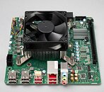
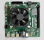
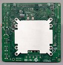
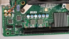
AMD 4700S SoC Desktop Motherboard Pictured

Pictures of the mysterious AMD 4700S SoC desktop kit just hit the web, courtesy Disclosuzen. As we reported earlier, the 4700S could be derived from the semi-custom SoC AMD originally co-developed with Microsoft for the Xbox Series X/S consoles. Close-ups of the PC motherboard reveals an interesting aspect—the board lacks any discernible display output, and instead relies on a PCI-Express graphics card. The board is built in the Mini-ITX form-factor, and draws power from a conventional combination of 24-pin ATX and 8-pin EPS power connectors.

A custom-design fan-heatsink cools the SoC. There are no memory slots, an unknown amount of hardwired memory under the SoC heatsink. 6-channel HD audio, wired Ethernet, and twelve USB ports (six each of USB 3.x and USB 2.0), make for the rest of the I/O. Storage connectivity is interesting—there are no M.2 NVMe slots, just two SATA ports. Why AMD even came up with this contraption is anyone's guess, but we guess it serves two purposes—1, it lets AMD harvest dies with faulty iGPUs, and 2, it serves as a decent developer platform, for game devs to at least optimize for the CPU. The lack of any NVMe storage interfaces points to the likelihood of this board not being meant for the general audience. Retail channel availability of the board seems unlikely, although it won't surprise us if suppliers on AliExpress list it anyway.

Apple M1 Processor Receives Preliminary Support in Linux Kernel

Apple's M1 custom processor has been widely adopted among the developer community. However, it is exactly this part of the M1 customer base that wants something different. For months, various developers have been helping with the adoption of the M1 processor for the Linux Kernel, which has today received preliminary support for the processor. The latest 5.13-RC1 release of the Linux Kernel is out, and it adds some basic functionality for the M1 processor. For now, it is some basic stuff like a simple bring up, however, much more has to be added. For example, the GPU support is still not done. Not even half-done. The M1 SoC is now able to boot, however, it takes a lot more work to get the full SoC working correctly.

Mr. Linus Torvalds, the Linux kernel developer, and its creator highlights that "This was - as expected - a fairly big merge window, but things seem to have proceeded fairly smoothly. Famous last words." According to one of the main activists for Linux on M1, Mr. Hector Martin, "This is just basic bring-up, but it lays a solid foundation and is probably the most challenging up-streaming step we'll have to do, at least until the GPU stuff is done." So it is still a long way before the M1 processor takes a full Linux kernel for a spin and the software becomes usable.

Samsung's Apple M1-rivaling Exynos SoC Powering Notebooks by H2-2021

Samsung is readying a powerful Arm-based SoC rivaling Apple's groundbreaking M1 silicon, under its Exynos brand. This chip is being designed for thin-and-light notebooks, as well as premium tablets, essentially letting Samsung target Apple's MacBook (M1) and iPad Pro form-factors. Unlike Apple, Samsung won't be burdened with having to rally its ISV partners to develop specifically for its hardware; the company is preparing to launch notebooks in the second half of 2021 that are powered by a Windows 10 on Arm derivative. This would give the notebook access to all of the applications already developed for the OS, including Office and certain Adobe Creativity Suite apps. The M1-rivaling Exynos chip will pack the latest-generation 64-bit Arm CPU cores, as well as an integrated GPU designed by AMD.

Xilinx Reports Fiscal Fourth Quarter and Fiscal Year 2021 Results

Xilinx, Inc. (Nasdaq: XLNX), the leader in adaptive computing, today announced record revenues of $851 million for the fiscal fourth quarter, up 6% over the previous quarter and an increase of 13% year over year. Fiscal 2021 revenues were $3.15 billion, largely flat from the prior fiscal year. GAAP net income for the fiscal fourth quarter was $188 million, or $0.75 per diluted share. Non-GAAP net income for the quarter was $204 million, or $0.82 per diluted share. GAAP net income for fiscal year 2021 was $647 million, or $2.62 per diluted share. Non-GAAP net income for fiscal year 2021 was $762 million, or $3.08 per diluted share.

Additional fourth quarter of fiscal year 2021 comparisons are provided in the charts below. "We are pleased with our fourth quarter results as we delivered record revenues and double-digit year-over-year growth in the midst of a challenging supply chain environment," said Victor Peng, Xilinx president and CEO. "Xilinx saw further improvement in demand across a majority of our diversified end markets with key strength in our Wireless, Data Center and Automotive markets, the pillars of our growth strategy. Our teams have executed well and we remain focused on continuing to meet customers' critical needs.

Intel NUC 11 Essential Detailed: Powered by Pentium Silver and Celeron "Jasper Lake"

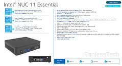
Intel is giving finishing touches to the NUC 11 Essential, its next-generation entry-level NUC desktops powered by Pentium Silver and Celeron SoCs based on the 10 nm "Jasper Lake" silicon. Among the SoC options are the Pentium Silver J6005, packing a 4-core/4-thread CPU based on the "Tremont" microarchitecture, a Gen11 iGPU with 32 execution units, and a dual-channel DDR4 memory interface. The Celeron J5105 is the next best option, with slightly lower clock speeds, and the Celeron J4505, a 2-core/2-thread part.

The NUC 11 Essential comes with two DDR4 SO-DIMM slots supporting up to 16 GB of dual-channel DDR4-2933 memory. The Gen11 iGPU is leveraged to put out an HDMI 2.0b port, and a DisplayPort 1.4, both of which support 4K displays up to 60 Hz. Connectivity includes 802.11ax + Bluetooth 4.2 with audio offload; 1 GbE wired LAN, four 5 Gbps USB 3.1 type-A ports, and two USB 2.0 ports.A 65-Watt power brick is included. It measures 135 mm x 115 mm x 36 mm.

Apple M2 Processor is Reportedly in Mass Production

Apple's M1 processors are a big success. When Apple introduced the M1 processors in the MacBook lineup, everyone was impressed by the processor performance and the power efficiency it offered. Just a few days ago, Apple updated its Mac lineup to feature these M1 processors and made it obvious that custom silicon is the way to go in the future. Today, we have information coming from Nikkei Asia, that Apple's next-generation M2 chip has entered mass production and that it could be on the way for as early as July when Apple will reportedly refresh its products. The M2 chip is made inside TSMC's facilities on a 5 nm+ N5P node. While there is no more information coming from the report about the SoC, we can expect it to be a good generational improvement.

Arm Announces Neoverse N2 and V1 Server Platforms

The demands of data center workloads and internet traffic are growing exponentially, and new solutions are needed to keep up with these demands while reducing the current and anticipated growth of power consumption. But the variety of workloads and applications being run today means the traditional one-size-fits all approach to computing is not the answer. The industry demands flexibility; design freedom to achieve the right level of compute for the right application.

As Moore's Law comes to an end, solution providers are seeking specialized processing. Enabling specialized processing has been a focal point since the inception of our Neoverse line of platforms, and we expect these latest additions to accelerate this trend.

Tenstorrent Selects SiFive Intelligence X280 for Next-Generation AI Processors

SiFive, Inc., the industry leader in RISC-V processors and silicon solutions, today announced that Tenstorrent, an AI semiconductor and software start-up developing next-generation computers, will license the new SiFive Intelligence X280 processor in its AI training and inference processor. SiFive will deliver more details of its SiFive Intelligence initiative including the SiFive Intelligence X280 processor at the Linley Spring Processor Conference on April 23rd.

Tenstorrent's novel approach to inference and training effectively and efficiently accommodates the exponential growth in the size of machine learning models while offering best-in-class performance.

UK Stalls NVIDIA's Acquisition of Arm to Investigate "National Security Concerns"

The UK government has stalled NVIDIA's $40 billion acquisition of Arm by constituting an investigation in "public interest." This investigation will look into the national security implications to the UK, of the acquisition. Although Arm is being transacted between Japan's SoftBank Holdings and American NVIDIA, Arm itself is a UK-based entity. The Competition and Markets Authority (CMA) will lead the investigation, and file a report with the UK government by June 30, 2021.

NVIDIA responded to the development, stating that the acquisition has no material national-security issues affecting the UK. "We will continue to work closely with the British authorities, as we have done since the announcement of this deal," NVIDIA stated. Leading tech firms, namely Google, Qualcomm, and Microsoft, etc., voiced apprehensions over the deal. Unlike SoftBank, NVIDIA is a chip-designer in its own right, and could withhold cutting-edge Arm technology to itself, giving its CPUs/SoCs a competitive edge over other Arm licensees, these firms believe.

OpenFive Tapes Out SoC for Advanced HPC/AI Solutions on TSMC 5 nm Technology

OpenFive, a leading provider of customizable, silicon-focused solutions with differentiated IP, today announced the successful tape out of a high-performance SoC on TSMC's N5 process, with integrated IP solutions targeted for cutting edge High Performance Computing (HPC)/AI, networking, and storage solutions.

The SoC features an OpenFive High Bandwidth Memory (HBM3) IP subsystem and D2D I/Os, as well as a SiFive E76 32-bit CPU core. The HBM3 interface supports 7.2 Gbps speeds allowing high throughput memories to feed domain-specific accelerators in compute-intensive applications including HPC, AI, Networking, and Storage. OpenFive's low-power, low-latency, and highly scalable D2D interface technology allows for expanding compute performance by connecting multiple dice together using an organic substrate or a silicon interposer in a 2.5D package.

TSMC to Enter 4 nm Node Volume Production in Q4 of 2021

TSMC, the world leader in semiconductor manufacturing, has reportedly begun with plans to start volume production of the 4 nm node by the end of this year. According to the sources over at DigiTimes, Taiwan's leading semiconductor manufacturer could be on the verge of starting volume production of an even smaller node. The new 4 nm node is internally referred to as a part of the N5 node generation. The N5 generation covers N5 (regular 5 nm), N5P (5 nm+), and N4 process that is expected to debut soon. And perhaps the most interesting thing is that the 4 nm process will be in high-volume production in Q4, with Apple expected to be one of the major consumers of the N5 node family.

DigiTimes reports that Apple will use the N5P node for the upcoming Apple A15 SoCs for next-generation iPhones, while the more advanced N4 node will find itself as a base of the new Macs equipped with custom Apple Silicon SoCs. To find out more, we have to wait for the official product launches and see just how much improvement new nodes bring.

Revenue of Top 10 IC Design (Fabless) Companies for 2020 Undergoes 26.4% Increase YoY, Says TrendForce

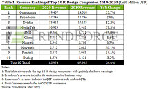
The emergence of the COVID-19 pandemic in 1H20 seemed at first poised to devastate the IC design industry. However, as WFH and distance education became the norm, TrendForce finds that the demand for notebook computers and networking products also spiked in response, in turn driving manufacturers to massively ramp up their procurement activities for components. Fabless IC design companies that supply such components therefore benefitted greatly from manufacturers' procurement demand, and the IC design industry underwent tremendous growth in 2020. In particular, the top three IC design companies (Qualcomm, Broadcom, and Nvidia) all posted YoY increases in their revenues, with Nvidia registering the most impressive growth, at a staggering 52.2% increase YoY, the highest among the top 10 companies.

Next-Generation Nintendo Switch SoC to be Powered by NVIDIA's Ada Lovelace GPU Architecture

Nintendo's Switch console is one of the most successful consoles ever made by the Japanese company. It has sold in millions of units and has received great feedback from the gaming community. However, as the hardware inside the console becomes outdated, the company is thinking about launching a new revision of the console, with the latest hardware and technologies. Today, we got ahold of information about the graphics side of things in Nintendo's upcoming console. Powered by NVIDIA Tegra SoC, it will incorporate unknown Arm-based CPU cores. The latest rumors suggest that the CPU will be accommodated with NVIDIA's Ada Lovelace GPU architecture. According to @kopite7kimi, a known hardware leaker, who simply replied to VideoCardz's tweet with "Ada", we are going to see the appearance of Ada Lovelace GPU architecture in the new SoC. Additionally, the new Switch SoC will have hardware accelerated NVIDIA Deep Learning Super Sampling (DLSS) and 4K output.

Google Hires Intel Veteran Uri Frank To Lead Datacenter SoC Development

Google has recently hired Intel veteran Uri Frank as VP of Engineering for the newly created server chip design division. The new division will develop custom Systems on Chip for use in Google datacenters to gain higher performance and to use less power by integrating hardware and software. Google has considerable experience in hardware development starting with its Tensor Processing Unit in 2015, its Video Processing Units in 2018, and in 2019 he first open-source silicon root-of-trust project. Google has also developed custom hardware solutions for SSDs, HDDs, network switches, and network interface cards in collaboration with external partners.

Google hopes to reduce the latency and bandwidth between different components by integrating them all into custom SoCs to improve power consumption and cost compared to individual ASICs on a motherboard. The development of these custom SoCs will be a long one with Google planning to hire hundreds of SoC engineers so we will be waiting a few years before we begin to see these deployed. This move is consistent with rivals Amazon Web Services and Microsoft Azure who are both also developing custom server chips for their datacenters. Google will continue to purchase existing productions where it is more practical to do so and hopes to create an ecosystem that will benefit the entire industry.

ECS Announces LIVA M300-W Industrial-grade Mini PC

Elitegroup Computer Systems (ECS), the global leading motherboard, Mini-PC, Notebooks, mobile device and smart city solutions provider, is proud to present the latest light and thin mini PC - LIVA M300-W. LIVA M300-W is designed by iron grey metal chassis with compact size measuring only 12.8 x 12.8 x 2.6 cm. LIVA M300-W is powered by Rockchip RK3399K SoC with quad and dual core CPU which can support dual operating system of Android 8.1 and Lubuntu 18.04. It is also equipped with HDMI 2.0 port which can support up to 4K resolution and CEC system. LIVA M300-W is crafted for industrial use by its wide temperature and dustproof design. It is an ideal mini PC to run under extreme environment such as construction site, factory and warehouse for many applications like surveillance, terminal, POS and thermal-sensing.

LIVA M300-W features the outstanding fanless thermal design. It can effectively dissipate heat and operate in wide-temperature from -10°C to 60°C and humidity range from 10% to 95% when CPU running multi-tasks stably under critical environment such as construction site, casino, transportation center and shopping mall.

GLOBALFOUNDRIES 22FDX RF Solution Provides the Basis for Next-Gen mmWave Automotive Radar

GLOBALFOUNDRIES (GF ), the global leader in specialty semiconductor manufacturing, and Bosch will partner to develop and manufacture next-generation automotive radar technology.

Bosch chose GF as its partner to develop a mmWave automotive radar system-on-chip (SoC) for Advanced Driver Assistance Systems (ADAS) applications, manufactured using GF's 22FDX RF solution. ADAS applications help drivers stay safe by keeping a vehicle in the correct lane, warning of collisions, initiating emergency braking, assisting with parking, and more.

SiPearl to Manufacture its 72-Core Rhea HPC SoC at TSMC Facilities

SiPearl has this week announced their collaboration with Open-Silicon Research, the India-based entity of OpenFive, to produce the next-generation SoC designed for HPC purposes. SiPearl is a part of the European Processor Initiative (EPI) team and is responsible for designing the SoC itself that is supposed to be a base for the European exascale supercomputer. In the partnership with Open-Silicon Research, SiPearl expects to get a service that will integrate all the IP blocks and help with the tape out of the chip once it is done. There is a deadline set for the year 2023, however, both companies expect the chip to get shipped by Q4 of 2022.

When it comes to details of the SoC, it is called Rhea and it will be a 72-core Arm ISA based processor with Neoverse Zeus cores interconnected by a mesh. There are going to be 68 mesh network L3 cache slices in between all of the cores. All of that will be manufactured using TSMC's 6 nm extreme ultraviolet lithography (EUV) technology for silicon manufacturing. The Rhea SoC design will utilize 2.5D packaging with many IP blocks stitched together and HBM2E memory present on the die. It is unknown exactly what configuration of HBM2E is going to be present. The system will also see support for DDR5 memory and thus enable two-level system memory by combining HBM and DDR. We are excited to see how the final product looks like and now we wait for more updates on the project.

Samsung is Preparing Exynos SoC with Radeon GPU for Next-Generation PCs

In 2019, AMD and Samsung have announced that they will be joining forces to develop a new class of mobile SoCs, carrying the Exynos name and having a Radeon GPU inside. These Exynos SoCs could be used for almost everything that needs a low-power processor. While the original plan was to have these processors run inside Samsung's mobile phone offerings, it seems like there is another application for them. If the rumors coming from ZDNet Korea are correct, we are in for a surprise. According to the source, Samsung is preparing to use the Exynos SoC with Radeon graphics in the company's next-generation laptops lineup.

While there is little to no information regarding the specifications of the said system, we can expect it to be a fully Samsung-made laptop. That means that Samsung will provide display, RAM, storage, battery, and other components manufactured by the company or its divisions. This laptop is expected to replace Samsung's Galaxy Book S, which currently uses Qualcomm Snapdragon 8cx SoC. The new PC is going to be Windows 10 based system. For more details, we have to wait for the announcement.

Sony Playstation 5 SoC Die Has Been Pictured

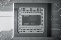
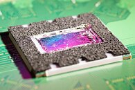
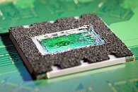
When AMD and Sony collaborated on making the next generation console chip, AMD has internally codenamed it Flute, while Sony codenamed it Oberon or Ariel. This PlayStation 5 SoC die has today been pictured thanks to the Fritzchens Fritz and we get to see a closer look at the die internals. Featuring eight of AMD's Zen2 cores that can reach frequencies of up to 3.5 GHz, the CPU is paired with 36 CU GPU based on the RDNA 2 technology. The GPU is capable of running at speed of up to 2.23 GHz. The SoC has been made to accommodate all of that hardware, and bring IO to connect it all.

When tearing down the console, the heatsink and the SoC are connected by liquid metal, which is used to achieve the best possible heat transfer between two surfaces. Surrounding the die there is a small amount of material used to prevent liquid metal (a conductive material) from possibly spilling and shorting some components. Using a special short wave infrared light (SWIR) microscope, we can take a look at what is happening under the hood without destroying the chip. And really, there are a few distinct areas that are highlighted by the Twitter user @Locuza. As you can see, the die has special sectors with the CPU complex and a GPU matrix with plenty of workgroups and additional components for raytracing.

Xilinx Collaborates with Fujitsu to Support 5G Deployments in the US

Xilinx, Inc.,, the leader in adaptive computing, today announced that the company is supplying its leading UltraScale+ technology to Fujitsu Limited for its O-RAN 5G radio units (O-RUs). Fujitsu O-RUs using Xilinx technology will be deployed in the first O-RAN-compliant 5G greenfield networks in the U.S. Fujitsu is also evaluating Xilinx RFSoC technology to further reduce cost and power consumption for additional future site deployments.

Fujitsu O-RUs are ideal for a broad-range of spectrum and multi-band applications for 5G O-RAN networks. The Xilinx UltraScale+ devices used within Fujitsu O-RUs deliver the best balance of cost economies as well as the adaptability and scalability required for the evolving needs of 5G O-RAN network requirements. Additionally, Xilinx will continue to work with other O-RAN ecosystem partners to ensure continued validation of the hardware and software necessary for world-class 5G networks.

Samsung Exynos SoC with AMD RDNA GPU Destroys Competition, Apple 14 Bionic SoC Kneels

Some time ago, Samsung and AMD announced that they will be building a mobile processor that utilizes AMD RDNA architecture for graphics processing. Samsung is readying its Exynos 2100 SoC and today we get to see its performance results in the first leaked benchmark. The new SoC design has been put through a series of GPU-only benchmarks that stress just the AMD RDNA GPU. Firstly there is Manhattan 3 benchmark where the Exynos SoC scored 181.8 FPS. Secondly, the GPU has scored 138.25 FPS in Aztek Normal and 58 FPS in Aztek High. If we compare those results to the Apple A14 Bionic chip, which scored 146.4 FPS in Manhattan 3, 79.8 FPS in Aztek Normal, and 30.5 FPS in Aztek High, the Exynos design is faster anywhere from 25% to 100%. Of course, given that this is only a leak, all information should be taken with a grain of salt.
Return to Keyword Browsing
Apr 25th, 2024 13:13 EDT change timezone

New Forum Posts

Popular Reviews

Controversial News Posts