News Posts matching #Sunny Cove

Return to Keyword Browsing

Intel "Tiger Lake" Architecture Combines Willow Cove CPU Cores and Xe iGPU

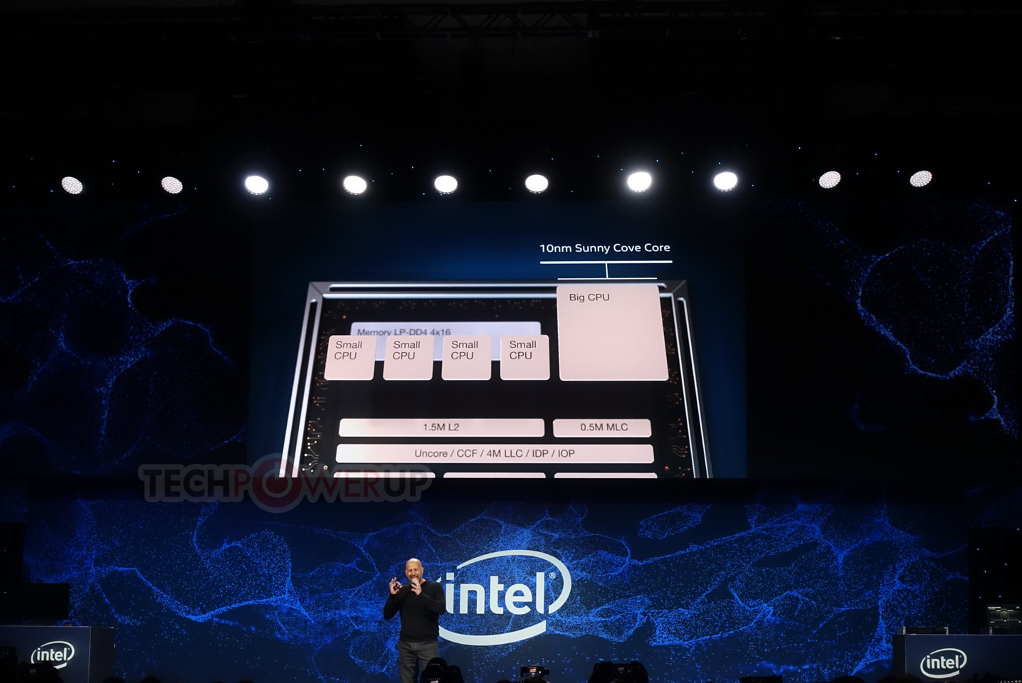
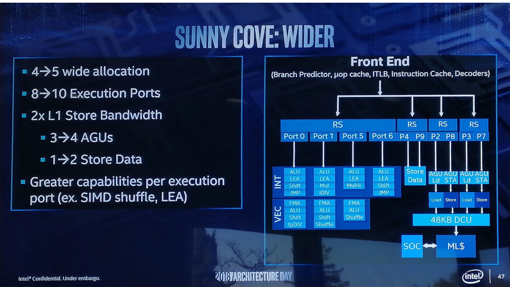
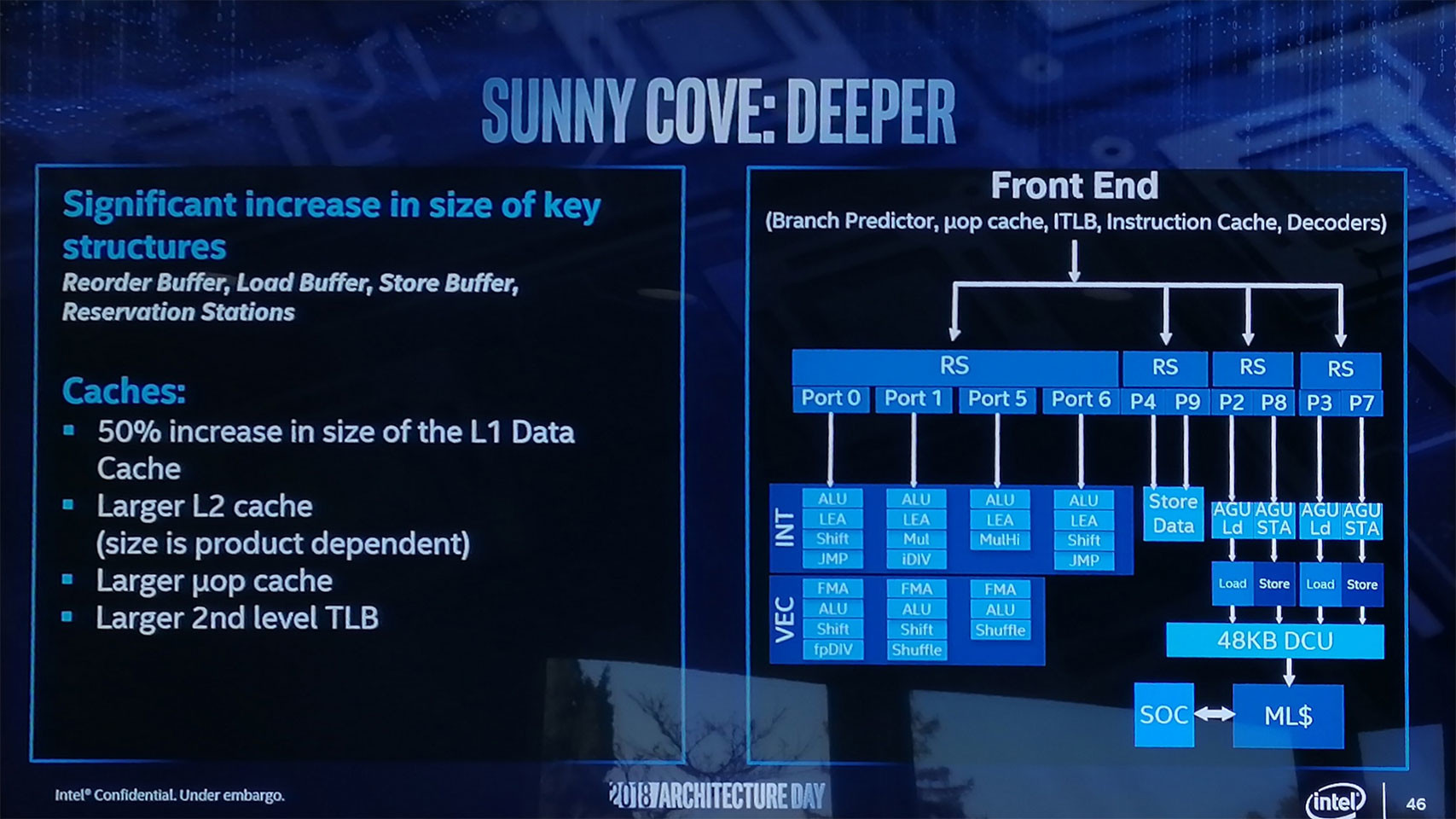
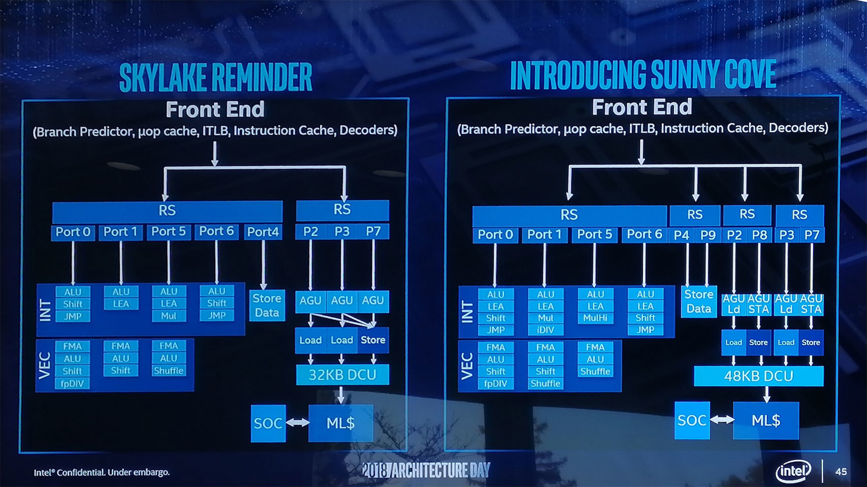
Even as Intel banks on 10 nm "Ice Lake" to pull it out of the 14 nm dark ages, the company is designing a fascinating new monolithic processor SoC die that succeeds it. Codenamed "Tiger Lake," and slated to debut in 2020, this die packs "Willow Cove" CPU cores and an iGPU based on Intel's Xe architecture, not Gen11. "Willow Cove" CPU cores are more advanced than the "Sunny Cove" cores "Ice Lake" packs, featuring a redesigned on-die cache, additional security features, and transistor optimization yielded from the newer 10 nm+ silicon fabrication process.

Intel is already boasting of 1 TFLOP/s compute power of the Gen11 iGPU on "Ice Lake," so it's logical to predict that the Xe based iGPU will be significantly faster. It will also support the latest display standards. The "next-gen I/O" referenced by Intel could be faster NVMe, Thunderbolt, and USB standards that leverage the bandwidth doubling brought about by PCI-Express gen 4.0. Here's the catch: much like "Ice Lake," the new "Tiger Lake" chip will get a mobile debut as Tiger Lake-Y or Tiger Lake-U, and desktop processors could follow later, possibly even 2021, depending on how much pressure it faces from AMD.

Intel Switches Gears to 7nm Post 10nm, First Node Live in 2021

Intel's semiconductor manufacturing business has had a terrible past 5 years as it struggled to execute its 10 nanometer roadmap forcing the company's processor designers to re-hash the "Skylake" microarchitecture for 5 generations of Core processors, including the upcoming "Comet Lake." Its truly next-generation microarchitecture, codenamed "Ice Lake," which features a new CPU core design called "Sunny Cove," comes out toward the end of 2019, with desktop rollouts expected 2020. It turns out that the 10 nm process it's designed for, will have a rather short reign at Intel's fabs. Speaking at an investor's summit on Wednesday, Intel put out its silicon fabrication roadmap that sees an accelerated roll-out of Intel's own 7 nm process.

When it goes live and fit for mass production some time in 2021, Intel's 7 nm process will be a staggering 3 years behind TSMC, which fired up its 7 nm node in 2018. AMD is already mass-producing CPUs and GPUs on this node. Unlike TSMC, Intel will implement EUV (extreme ultraviolet) lithography straightaway. TSMC began 7 nm with DUV (deep ultraviolet) in 2018, and its EUV node went live in March. Samsung's 7 nm EUV node went up last October. Intel's roadmap doesn't show a leap from its current 10 nm node to 7 nm EUV, though. Intel will refine the 10 nm node to squeeze out energy-efficiency, with a refreshed 10 nm+ node that goes live some time in 2020.

Intel 10nm Ice Lake to Quantitatively Debut Within 2019

Intel put out interesting details about its upcoming 10 nanometer "Ice Lake" CPU microarchitecture rollout in its recent quarterly financial results call. The company has started qualification of its 10 nm "Ice Lake" processors. This involves sending engineering samples to OEMs, system integrators and other relevant industry partners, and getting the chips approved for their future product designs. The first implementation of "Ice Lake" will not be a desktop processor, but rather a low-power mobile SoC designed for ultraportables, codenamed "Ice Lake-U." This SoC packs a 4-core/8-thread CPU based on the "Sunny Cove" core design, and Gen11 GT2 integrated graphics with 64 execution units and nearly 1 TFLOP/s compute power. This SoC will also support WiFi 6 and LPDDR4X memory.

Intel CEO Bob Swan also remarked that the company has doubled its 10 nm yield expectations. "On the [10 nm] process technology front, our teams executed well in Q1 and our velocity is increasing," he said, adding "We remain on track to have volume client systems on shelves for the holiday selling season. And over the past four months, the organization drove a nearly 2X improvement in the rate at which 10nm products move through our factories." Intel is prioritizing enterprise over desktop, as "Ice Lake-U" will be followed by "Ice Lake-SP" Xeon rollout in 2020. There was no mention of desktop implementations such as "Ice Lake-S." Intel is rumored to be preparing a stopgap microarchitecture for the desktop platform to compete with AMD "Matisse" Zen 2 AM4 processors, codenamed "Comet Lake." This is essentially a Skylake 10-core die fabbed on existing 14 nm++ node. AMD in its CES keynote announced an achievement of per-core performance parity with Intel, so it could be interesting to see how Intel hopes 10 "Skylake" cores match up to 12-16 "Zen 2" cores.

Intel Unveils "Lakefield" Heterogenous SoC and "Project Athena"

Intel today unveiled a killer new product with which it hopes to bring about as big a change to mobile computing as Ultrabook did some eight years ago. This effort is a combination of a new mobile computing form-factor codenamed "Project Athena," and an SoC at its heart, codenamed "Lakefield." Put simply, "Lakefield" is a 10 nm SoC that's integrated much in the same way as today's ARM SoCs, which combine IP from various vendors onto a single PoP (package-over-package) Foveros die.

The biggest innovation with "Lakefield" is its hybrid x86 multi-core CPU design, which combines four Atom-class low-power cores, with one Core-class "Sunny Cove" core, in a setup akin to ARM's big.LITTLE. Low-power processing loads are distributed to the smaller cores, while the big core is woken up to deal with heavy loads. The SoC also integrates a Gen 11 iGPU core, partial components to accelerate 802.11ax WLAN, 5G, an PoP DRAM and NVMe storage devices. The reference motherboard based on "Lakefield" is barely larger than an M.2 SSD!

Intel's Foveros-based, Hybrid x86 CPUs Mean the Company Needed to Sprinkle some ARM

Intel at its architecture day revealed one of the more exquisite in-house designs for the company in recent years: a hybrid x86 chip that seems to imbibe from ARM's own big.Little design mantra. The new Hybrid x86 CPU that was announced takes this design choice in pairing a single, high-performance Sunny Cove core with four smaller Atom cores. This chip is built using Intel's Foveros manufacturing technology, which means a 22FFL IO chip serves as an active interposer, connected via TSVs to a 10nm die that contains both types of cores. The tiny chips measures just 12 x 12 x 1 mm (144 mm²), and looks to reduce footprint even further by including a POP (package on package) memory design.

The new Intel design is aimed at low-power environments, with the chip having been designed to work on a 2 mW standby power ratio, with less than a 7 W of power - for a big.Little five-core design and a 64 EU design with Gen11 graphics core. Intel's Jim Keller said that the company is testing the intricacies and advantages of this design internally, so more products based on this manufacturing and packaging mantra could pop up sometime in the future.

Intel 10nm "Ice Lake" to Combine "Sunny Cove" CPU Cores with Gen11 iGPU

Intel's upcoming "Ice Lake" die could be the company's biggest processor innovation in a decade, combining new clean-slate design "Sunny Cove" CPU cores, and a new integrated graphics solution based on the company's Gen11 architecture. "Sunny Cove" introduces significant IPC (single-thread performance) gains over "Coffee Lake," introduces new ISA instruction sets, including AVX-512; and a brand new uncore component; while the Gen11 graphics core is Intel's first iGPU to reach the 1 TFLOP/s mark. Intel demonstrated the ultra-low power "Ice Lake-U" SoC platform in its 2018 Architecture Day briefing.

This "Ice Lake-U" chip, with its TDP in the ballpark of 15 W, was shown ripping through 7-zip and "Tekken 7." With 7-zip, Intel was trying to demonstrate vector-AES and SHA-NI improving archive encryption performance by 75 percent over "Skylake." The Gen11 iGPU was shown providing a smoother gameplay than Skylake with Gen9, although the company neither mentioned resolution, nor frame-rates. Anandtech wagers it's above 30 fps.

Intel Unveils a Clean-slate CPU Core Architecture Codenamed "Sunny Cove"

Intel today unveiled its first clean-slate CPU core micro-architecture since "Nehalem," codenamed "Sunny Cove." Over the past decade, the 9-odd generations of Core processors were based on incrementally refined descendants of "Nehalem," running all the way down to "Coffee Lake." Intel now wants a clean-slate core design, much like AMD "Zen" is a clean-slate compared to "Stars" or to a large extent even "Bulldozer." This allows Intel to introduce significant gains in IPC (single-thread performance) over the current generation. Intel's IPC growth curve over the past three micro-architectures has remained flat, and only grew single-digit percentages over the generations prior.

It's important to note here, that "Sunny Cove" is the codename for the core design. Intel's earlier codenaming was all-encompassing, covering not just cores, but also uncore, and entire dies. It's up to Intel's future chip-designers to design dies with many of these cores, a future-generation iGPU such as Gen11, and a next-generation uncore that probably integrates PCIe gen 4.0 and DDR5 memory. Intel details "Sunny Cove" as far as mentioning IPC gains, a new ISA (new instruction sets and hardware capabilities, including AVX-512), and improved scalability (ability to increase core-counts without running into latency problems).
Return to Keyword Browsing
Apr 25th, 2024 11:39 EDT change timezone

New Forum Posts

Popular Reviews

Controversial News Posts