News Posts matching #TSMC

Return to Keyword Browsing

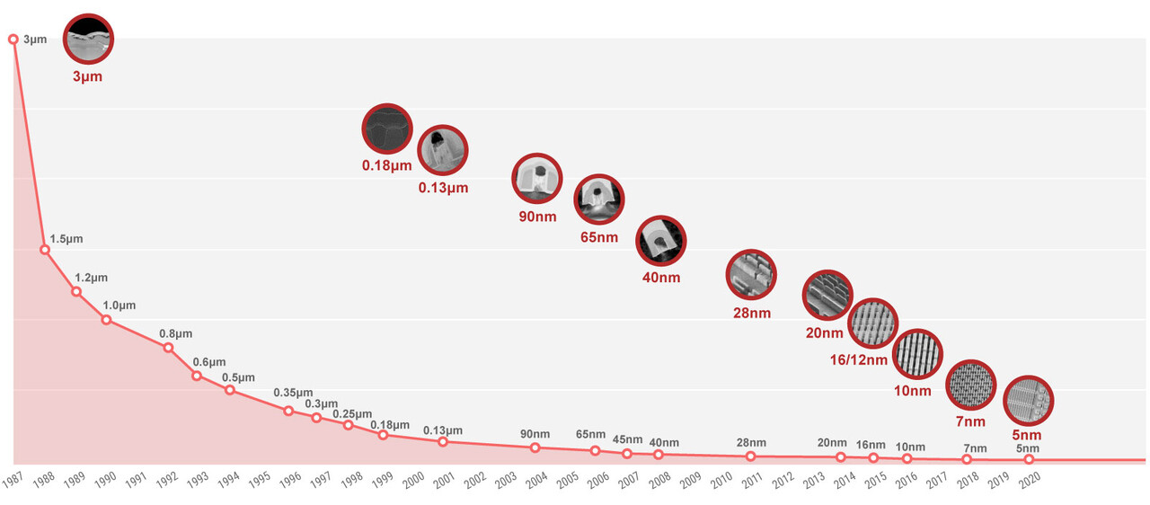
TSMC to Start 2 nm Production by 2025, 3 nm by the End of 2022

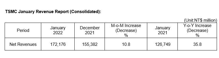
Responding to investor questions in TSMC's first quarter earnings call for 2022, CEO C. C. Wei reiterated that the company's upcoming manufacturing processes are generally moving smoothly throughout development. Even as TSMC announced historic revenues on the back of increased pricing throughout the semiconductor industry, the company is showing no signs of slowing down on its development. When further asked regarding the company's ability to navigate the world's troubled, inflation-ridden waters, Wei added that TSMC's strategic positioning as the leading semiconductor foundry makes it resilient to market and demand fluctuations.

TSMC's roadmap has seen multiple accelerations of late, which have placed 3 nm tape-out to occur before the end of the year. Perhaps more significantly, the company's next-generation 2 nm manufacturing process, which will make use of GAA (Gate All Around) transistor designs for greater design efficiency and density, are still on track for a 2025 volume production following an expected 2024 tape-out.

Alibaba Previews Home-Grown CPUs with 128 Armv9 Cores, DDR5, and PCIe 5.0 Technology

One of the largest cloud providers in China, Alibaba, has today announced a preview for a new instance powered by Yitian 710 processor. The new processor is a collection of Alibaba's efforts to develop a home-grown design capable of powering cloud instances and the infrastructure needed for it and its clients. Without much further ado, the Yitian 710 is based on Armv9 ISA and features 128 cores. Ramping up to 3.2 GHz, these cores are paired with eight-channel DDR5 memory to enable sufficient data transfer. In addition, the CPU supports 96 PCIe 5.0 lanes for IO with storage and accelerators. These are most likely custom designs, and we don't know if they are using a blueprint based on Arm's Neoverse. The CPU is manufactured at TSMC's facilities on 5 nm node and features 60 billion transistors.

Alibaba offers these processors as a part of their Elastic Compute Service (ECS) instance called g8m, where users can select 1/2/4/8/16/32/64/128 vCPUs, where each vCPU is equal to one CPU core physically. Alibaba is running this as a trial option and notes that users should not run production code on these instances, as they will disappear after two months. Only 100 instances are available for now, and they are based in Alibaba's Hangzhou zone in China. The company notes that instances based on Yitian 710 processors offer 100 percent higher efficiency than existing AMD/Intel solutions; however, they don't have any useful data to back it up. The Chinese cloud giant is likely trying to test and see if the home-grown hardware can satisfy the needs of its clients so that they can continue the path to self-sustainability.

TSMC First Quarter 2022 Financials Show 45.1% Increase in Revenues

A new quarter and another forecast shattering revenue report from TSMC, as the company beat analysts' forecasts by over US$658 million, with a total revenue for the quarter of US$17.6 billion and a net income of almost US$7.26 billion. That's an increase in net income of 45.1 percent or 35.5 percent in sales. Although the monetary figures might be interesting to some, far more interesting details were also shared, such as production updates about future nodes. As a followup on yesterday's news post about 3 nanometer nodes, the N3 node is officially on track for mass production in the second half of this year. TSMC says that customer engagement is stronger than at the start of its N7 and N7 nodes, with HPC and smartphone chip makers lining up to get onboard. The N3E node is, as reported yesterday, expected to enter mass production in the second half of 2023, or a year after N3. Finally, the N2 node is expected in 2025 and won't adhere to TSMC's two year process technology cadence.

Breaking down the revenue by nodes, N7 has taken back the lead over N5, as N7 accounted for 30 percent of TSMC's Q1 revenues up from 27 percent last quarter, but down from 35 percent in the previous year. N5 sits at 20 percent, which is down from 23 percent in the previous quarter, but up from 14 percent a year ago. The 16 and 28 nm nodes still hold on to 25 percent of TSMC's revenue, which is the same as a year ago and up slightly from the previous quarter. Remaining nodes are unchanged from last quarter.

TSMC's N3E Node Said to Have Good Yields, Volume Production Expected Q2 2023

Back in March there were reports of TSMC's N3E node having been moved from 2024 to the end of 2023. However, it seems like the node is already seeing better than expected yields and is now being pulled in further and TSMC is expecting to start volume production as early as Q2 in 2023. The node does appear to have been frozen when it comes to further development as of the end of March. Yields are said to be much higher than the N3B node, which is also under development, but with limited information available about it.

The first customer for the new node is expected to be Apple, as the company is largely paying for much of the cutting edge node development at TSMC. However, both Intel and Qualcomm are said to be some of the first customers for the new node. More details should hopefully be announced tomorrow during TSMC's first quarter earnings call. The N3E node is a reduced layer EUV process, but before it goes into mass production, it's likely we'll be seeing the N3 node first. Early production of 3 nm parts later this year is expected to be at around 10 to 20k wafers per month initially, rising to about 25 to 35k a month once TSMC's new fab is ready. Once the N3E node is in full swing, the monthly capacity of 3 nm parts should be around 50k wafers a month, but depending on customer demand, it might end up being even higher.

"Navi 31" RDNA3 Sees AMD Double Down on Chiplets: As Many as 7

Way back in January 2021, we heard a spectacular rumor about "Navi 31," the next-generation big GPU by AMD, being the company's first logic-MCM GPU (a GPU with more than one logic die). The company has a legacy of MCM GPUs, but those have been a single logic die surrounded by memory stacks. The RDNA3 graphics architecture that the "Navi 31" is based on, sees AMD fragment the logic die into smaller chiplets, with the goal of ensuring that only those specific components that benefit from the TSMC N5 node (6 nm), such as the number crunching machinery, are built on the node, while ancillary components, such as memory controllers, display controllers, or even media accelerators, are confined to chiplets built on an older node, such as the TSMC N6 (6 nm). AMD had taken this approach with its EPYC and Ryzen processors, where the chiplets with the CPU cores got the better node, and the other logic components got an older one.

Greymon55 predicts an interesting division of labor on the "Navi 31" MCM. Apparently, the number-crunching machinery is spread across two GCD (Graphics Complex Dies?). These dies pack the Shader Engines with their RDNA3 compute units (CU), Command Processor, Geometry Processor, Asynchronous Compute Engines (ACEs), Rendering Backends, etc. These are things that can benefit from the advanced 5 nm node, enabling AMD to the CUs at higher engine clocks. There's also sound logic behind building a big GPU with two such GCDs instead of a single large GCD, as smaller GPUs can be made with a single such GCD (exactly why we have two 8-core chiplets making up a 16-core Ryzen processors, and the one of these being used to create 8-core and 6-core SKUs). The smaller GCD would result in better yields per wafer, and minimize the need for separate wafer orders for a larger die (such as in the case of the Navi 21).

AMD EPYC "Genoa" Zen 4 Processor Multi-Chip Module Pictured

Here is the first picture of a next-generation AMD EPYC "Genoa" processor with its integrated heatspreader (IHS) removed. This is also possibly the first picture of a "Zen 4" CPU Complex Die (CCD). The picture reveals as many as twelve CCDs, and a large sIOD silicon. The "Zen 4" CCDs, built on the TSMC N5 (5 nm EUV) process, look visibly similar in size to the "Zen 3" CCDs built on the N7 (7 nm) process, which means the CCD's transistor count could be significantly higher, given the transistor-density gained from the 5 nm node. Besides more number-crunching machinery on the CPU core, we're hearing that AMD will increase cache sizes, particularly the dedicated L2 cache size, which is expected to be 1 MB per core, doubling from the previous generations of the "Zen" microarchitecture.

Each "Zen 4" CCD is reported to be about 8 mm² smaller in die-area than the "Zen 3" CCD, or about 10% smaller. What's interesting, though, is that the sIOD (server I/O die) is smaller in size, too, estimated to measure 397 mm², compared to the 416 mm² of the "Rome" and "Milan" sIOD. This is good reason to believe that AMD has switched over to a newer foundry process, such as the TSMC N7 (7 nm), to build the sIOD. The current-gen sIOD is built on Global Foundries 12LPP (12 nm). Supporting this theory is the fact that the "Genoa" sIOD has a 50% wider memory I/O (12-channel DDR5), 50% more IFOP ports (Infinity Fabric over package) to interconnect with the CCDs, and the mere fact that PCI-Express 5.0 and DDR5 switching fabric and SerDes (serializer/deserializers), may have higher TDP; which together compel AMD to use a smaller node such as 7 nm, for the sIOD. AMD is expected to debut the EPYC "Genoa" enterprise processors in the second half of 2022.

AMD Claims Radeon RX 6500M is Faster Than Intel Arc A370M Graphics

A few days ago, Intel announced its first official discrete graphics card efforts, designed for laptops. Called the Arc Alchemist lineup, Intel has designed these SKUs to provide entry-level to high-end options covering a wide range of use cases. Today, AMD has responded with a rather exciting Tweet made by the company's @Radeon Twitter account. The company compared Intel's Arc Alchemist A370M GPU with AMD's Radeon RX 6500M mobile SKUs in the post. These GPUs are made on TSMC's N6 node, feature 4 GB GDDR6 64-bit memory, 1024 FP32 cores, and have the same configurable TDP range of 35-50 Watts.

Below, you can see AMD's benchmarks of the following select games: Hitman 3, Total War Saga: Troy, F1 2021, Strange Brigade (High), and Final Fantasy XIV. The Radeon RX 6500M GPU manages to win in all of these games, thus explaining AMD's "FTW" hashtag on Twitter. Remember that these are vendor-supplied benchmarks runs, so we have to wait for some media results to surface.

Intel Arc DG2-512 Built on TSMC 6nm, Has More Transistors than GA104 and Navi 22

Some interesting technical specifications of the elusive two GPUs behind the Intel Arc "Alchemist" series surfaced. The larger DG2-512 silicon in particular, which forms the base for the Arc 5 and Arc 7 series, is interesting, in that it is larger in every way than the performance-segment ASICs from both NVIDIA and AMD. The table below compares the physical specs of the DG2-512, with the NVIDIA GA104, and the AMD Navi 22. This segment of GPUs has fairly powerful use-cases, including native 1440p gameplay, or playing at 4K with a performance enhancement—something Intel has, in the form of the XeSS.

The DG2-512 is built on the 6 nm TSMC N6 foundry node, the most advanced node among the three GPUs in this class. It has the highest transistor density of 53.4 mTr/mm², and the largest die-area of 406 mm², and the highest transistor-count of 21.7 billion. The Xe-HPG graphics architecture is designed for full DirectX 12 Ultimate feature support, and the DG2-512 dedicated hardware for ray tracing, as well as AI acceleration. The Arc A770M is the fastest product based on this silicon, however, it is a mobile GPU with aggressive power-management characteristic to the form-factor it serves. Here, the DG2-512 has an FP32 throughput of 13.5 TFLOPs, compared to 13.2 TFLOPs of the Navi 22 on the Radeon RX 6700 XT desktop graphics card, and the 21.7 TFLOPs of the GA104 that's maxed out on the GeForce RTX 3070 Ti desktop graphics card.

AMD Ryzen 7000 "Raphael" Zen 4 Processors Enter Mass-Production by April-May?

The next-generation AMD Ryzen 7000 "Raphael" desktop processors in the Socket AM5 package are rumored to enter mass-production soon, according to Greymon55 on Twitter, a reliable source with AMD leaks. Silicon fabrication of the chips may already be underway, as the source claims that packaging (placing the dies on the fiberglass substrate or package), will commence by late-April or early-May. "Raphael" is a multi-chip module of "Zen 4" CCDs fabricated on the TSMC N5 (5 nm) node, combined with a cIOD built on a yet-unknown node. A plant in China performs packaging.

It's hard to predict retail availability, but for the Ryzen 5000 "Vermeer" processors, this development milestone was reached in June 2020, with the first products hitting shelves 4 months later, in November. This was, however, in the thick of the pre-vaccine COVID-19 pandemic. The "Zen 4" CPU cores are expected to introduce an IPC increase, as well as higher clock speeds. Also on offer will be next-gen connectivity, including PCI-Express Gen 5 (including CPU-attached Gen 5 NVMe), and DDR5 memory. These processors will launch alongside Socket AM5 motherboards based on the new AMD 600 series chipsets.

TSMC Ramps up Shipments to Record Levels, 5/4 nm Production Lines at Capacity

According to DigiTimes, TSMC is working on increased its monthly shipments of finished wafers from 120,000 to 150,000 for its 5 nm nodes, under which 4 nm also falls. This is three times as much as what TSMC was producing just a year ago. The 4 nm node is said to be in full mass production now and the enhanced N4P node should be ready for mass production in the second half of 2022, alongside N3B. This will be followed by the N4X and N3E nodes in 2023. The N3B node is expected to hit 40-50,000 wafers initially, before ramping up from there, assuming everything is on track.

The report also mentions that TSMC is expecting a 20 percent revenue increase from its 28 to 7 nm nodes this year, which shows that even these older nodes are being heavily utilised by its customers. TSMC has what NVIDIA would call a demand problem, as the company simply can't meet demand at the moment, with customers lining up to be able to get a share of any additional production capacity. NVIDIA is said to have paid TSMC at least US$10 billion in advance to secure manufacturing capacity for its upcoming products, both for consumer and enterprise products. TSMC's top three HPC customers are also said to have pre-booked capacity on the upcoming 3 and 2 nm nodes, so it doesn't look like demand is going to ease up anytime soon.

NVIDIA Could Use Intel's Foundry Service for Chip Manufacturing

Yesterday, NVIDIA announced its next-generation Hopper architecture designed for data center applications and workloads. There is always a question of availability, as the previous period showed everyone that the supply chain is overbooked and semiconductors are in very high demand. During the Q&A press session today, NVIDIA's CEO, Jensen Huang, tried to answer as many questions as possible. However, an exciting topic arose regarding the potential collaboration with Intel. As a part of Intel's IDM 2.0 strategy, the company plans to offer its chip manufacturing capabilities to the third-party companies willing to make efforts and port their designs to Intel's semiconductor nodes. NVIDIA, one of the largest TSMC customers, could be a new Intel customer. Below, we compiled a few quotes that highlight Jensen Huang's opinions, taking the quotes from Tom's Hardware.
NVIDIA CEO Jensen HuangOur strategy is to expand our supply base with diversity and redundancy at every single layer. At the chip layer, at the substrate layer, the system layer, at every single layer. We've diversified the number of nodes, we've diversified the number of foundries, and Intel is an excellent partner of ours[…]. They're interested in us using their foundries, and we're very interested in exploring it. [...] I am encouraged by the work that is done at Intel, I think this is a direction they have to go, and we're interested in looking at their process technology. Our relationship with Intel is quite long; we work with them across a whole lot of different areas, every single PC, every single laptop, every single PC, supercomputer, we collaborate. [...] We have been working closely with Intel, sharing with them our roadmap long before we share it with the public, for years. Intel has known our secrets for years. AMD has known our secrets for years. We are sophisticated and mature enough to realize that we have to collaborate.[...] We share roadmaps, of course, under confidentiality and a very selective channel of communications. The industry has just learned how to work in that way.

Taiwan Rocked by 6.6 Earthquake, Causes no Serious Production Issues

At 01:41 in the morning of the 23rd of March, the southeast coast of Taiwan experienced a magnitude 6.6 earthquake in the ocean outside Hualien County. The quake was felt island wide and some of the factories that operate 24/7 evacuated staff as a precautionary measure. All affected companies claim to have resumed operations later the same day, after checking that no damage was caused by the quake. The southeast of Taiwan kept being hit by minor quakes for the rest of the night and day, with some being felt across the island.

TSMC and UMC both claimed that the quake had a minimal effect on production, although production equipment had gone into self-protect mode, which was largely the reason for no production issues taking place. Powerchip Semiconductor on the other hand had a two to three hour production loss and Vanguard International Semiconductor was reported saying they were checking for defects in their production. AU Optronics and Innolux were also saved by their various safeguards against earthquake damage and both companies were expecting to return to normal production shortly. Other companies are said to have reported issues with their production equipment, but no damage to the actual products they produce.

Top 10 Foundries Post Record 4Q21 Performance for 10th Consecutive Quarter at US$29.55B, Says TrendForce

The output value of the world's top 10 foundries in 4Q21 reached US$29.55 billion, or 8.3% growth QoQ, according to TrendForce's research. This is due to the interaction of two major factors. One is limited growth in overall production capacity. At present, the shortage of certain components for TVs and laptops has eased but there are other peripheral materials derived from mature process such as PMIC, Wi-Fi, and MCU that are still in short supply, precipitating continued fully loaded foundry capacity. Second is rising average selling price (ASP). In the fourth quarter, more expensive wafers were produced in succession led by TSMC and foundries continued to adjust their product mix to increase ASP. In terms of changes in this quarter's top 10 ranking, Nexchip overtook incumbent DB Hitek to clinch 10th place.

TrendForce believes that the output value of the world's top ten foundries will maintain a growth trend in 1Q22 but appreciation in ASP will still be the primary driver of said growth. However, since there are fewer first quarter working days in the Greater China Area due to the Lunar New Year holiday and this is the time when some foundries schedule an annual maintenance period, 1Q22 growth rate will be down slightly compared to 4Q21.

TSMC's Largest Customer Accounts for 26 Percent of Revenues

You're not going to get an award for guessing who TSMC's biggest customer is, but based on details in TSMC's latest earnings report, its biggest customer stands for no less than 26 percent of TSMC's total revenue. That's up a whole percentage in 2021 over 2020 and as you most likely have already guessed, that company should be Apple. TSMC doesn't, for obvious reasons, reveal who their customers are, but it's no secret that Apple is spending a lot of money with the company. TSMC had a consolidated revenue of NT$1.587 trillion (US$55.73 billion) in 2021, or up 18.53 percent from 2020. The second largest source of revenue for TSMC might surprise some, at least based on the kind of information that the usual analysts tend to claim in their reports.

Although second place in terms of revenue only accounts for another 10 percent of TSMC's total revenue, we're still looking at some serious money here. However, as both Qualcomm and NVIDIA departed for Samsung in 2021, second place is said to be taken by AMD, which might not have been everyone's first guess. Unsurprisingly, 64 percent of TSMC's revenue is coming from companies in the USA, with Taiwan being the second largest source of revenue at 12.8 percent. As far as the PRC is concerned, revenue is said to be down by 29.6 percent and only makes up 10.3 percent of TSMC's revenues for 2021. This is largely due to the US sanctions against Huawei, according to the Taipei Times. The 7 nm node is still the big money maker for TSMC, which pulled in over NT$440 billion, followed by the 5 nm node at over NT$262 billion. However, the 5 nm node revenue grew by 188 percent in 2021, while the 7 nm node only had a revenue growth of 11.5 percent.

TSMC Said to be Close to Completing N3E Node

TSMC is working on multiple N3 nodes, with at least N3, N3B and N3E currently being in development. N3 is scheduled for production in 2023, with the N3E node originally being scheduled for 2024, but it now looks like it will be ready ahead of schedule. The N3E node was meant to be an enhanced version of the N3 node, but it now seems to be more of an alternative node, based on fewer EUV layers, supposedly down from 25 to 21 layers, which would make it easier to manufacture. According to details via Morgan Stanley, the N3E node is said to be around eight percent less dense than the original N3 node, but still around 60 percent denser than the N5 node. For comparison, the N3 node was said to have 70 percent denser logic than the N5 node.

The report suggests that the N3E node might be finished by the end of this month, which means production could end up being pulled in by a whole quarter, from Q3'23 to Q2'23. The N3E node is said to "feature improved manufacturing process window with better performance, power and yield", so we might see the N3E node being used for future products by just about anyone that is looking at making high-performance silicon. The N3E node is also said to have higher yields than the N3B node, with N3B said to be an improved version of N3 for certain customers. Not much else is known about the N3B node at the moment.

TSMC R&D SVP Expects Chip Shortage to Persist Until 2024-2025

In an interview with IEEE Spectrum Dr. Y.J. Mii, Senior Vice President of Research and Development at TSMC, said that he believes that we're not going to see an end to the chip shortage until the next generation of fabs that are currently under construction, or will commence soon, come online in two to three years. Interestingly, Mii is apparently not putting the blame squarely at the pandemic as so many others have for the components shortage, but rather points towards the fact that chips are being used in just about every kind of product these days. This has in turn led to much higher demands for semiconductors, without the infrastructure to manufacture enough of them being in place.

He also believes the industry as a whole missed the fact that the demand for a wide range of semiconductors was growing as quickly as it has been over the past few years. On the upside, it seems like the semiconductor manufacturers have understood what's going on and they're investing heavily in making sure that they can meet demand, both in the near term and longer term. Interestingly, he also mentions how hard it is, even for a company like TSMC, to progress their nodes today. He's quoted saying "Before, we could achieve the next-generation node by fine-tuning the process, but now for every generation we must find new ways in terms of transistor architecture, materials, processes, and tools. In the past, it's pretty much been a major optical shrink, but that's no longer a simple trick." It looks like the semiconductor manufacturers are going to have to come up with some new, innovative ways to be able to keep making better and faster semiconductors in the not too distant future.

Qualcomm Said to be Moving to TSMC for 3 nm Chips

Although nothing has been officially confirmed by Qualcomm, it looks like the company will be moving away from Samsung for its 3 nm based chips, in favour of TSMC. The Elec also mentions that Qualcomm has moved some of its Snapdragon 8 Gen 1 production to TSMC, something that has already been hitting the rumour mill. The first batch of 4 nm Snapdragon 8 Gen 1 chips are said to already have entered the early stages of production. The main reason for the move is said to be poor yields by Samsung Foundry on its 4 nm node.

The yield rates are said to be a measly 35 percent for the Snapdragon 8 Gen 1, with Samsung's Exynos 2200 having even lower yields. This also helps explain why Samsung's mobile division has decided to limit the availability of its Exynos 2200 based phones to only a few regions. Apparently Qualcomm had to send staff over to Korea to help get the yields up to their current rate, but it's not hard to see why the company is shifting back to TSMC, as a 35 percent yield rate is simply not acceptable. Samsung is said to be auditing Samsung Foundry to find out what has gone wrong, as anything below 80-90 percent in terms of yield rate is simply not acceptable for mass production. Qualcomm will apparently continue to use Samsung Foundry for its 7 nm RF chips, where the yields must be within industry norms.

Intel Details Ponte Vecchio Accelerator: 63 Tiles, 600 Watt TDP, and Lots of Bandwidth

During the International Solid-State Circuits Conference (ISSCC) 2022, Intel gave us a more significant look at its upcoming Ponte Vecchio HPC accelerator and how it operates. So far, Intel convinced us that the company created Ponte Vecchio out of 47 tiles glued together in one package. However, the ISSCC presentation shows that the accelerator is structured rather interestingly. There are 63 tiles in total, where 16 are reserved for compute, eight are used for RAMBO cache, two are Foveros base tiles, two represent Xe-Link tiles, eight are HBM2E tiles, and EMIB connection takes up 11 tiles. This totals for about 47 tiles. However, an additional 16 thermal tiles used in Ponte Vecchio regulate the massive TDP output of this accelerator.

What is interesting is that Intel gave away details of the RAMBO cache. This novel SRAM technology uses four banks of 3.75 MB groups total of 15 MB per tile. They are connected to the fabric at 1.3 TB/s connection per chip. In contrast, compute tiles are connected at 2.6 TB/s speeds to the chip fabric. With eight RAMBO cache tiles, we get an additional 120 MB SRAM present. The base tile is a 646 mm² die manufactured in Intel 7 semiconductor process and contains 17 layers. It includes a memory controller, the Fully Integrated Voltage Regulators (FIVR), power management, 16-lane PCIe 5.0 connection, and CXL interface. The entire area of Ponte Vecchio is rather impressive, as 47 active tiles take up 2,330 mm², whereas when we include thermal dies, the total area jumps to 3,100 mm². And, of course, the entire package is much larger at 4,844 mm², connected to the system with 4,468 pins.

Intel "Meteor Lake" and "Arrow Lake" Use GPU Chiplets

Intel's upcoming "Meteor Lake" and "Arrow Lake" client mobile processors introduce an interesting twist to the chiplet concept. Earlier represented in vague-looking IP blocks, new artistic impressions of the chip put out by Intel shed light on a 3-die approach not unlike the Ryzen "Vermeer" MCM that has up to two CPU core dies (CCDs) talking to a cIOD (client IO die), which handles all the SoC connectivity; Intel's design has one major difference, and that's integrated graphics. Apparently, Intel's MCM uses a GPU die sitting next to the CPU core die, and the I/O (SoC) die. Intel likes to call its chiplets "tiles," and so we'll go with that.

The Graphics tile, CPU tile, and the SoC or I/O tile, are built on three different silicon fabrication process nodes based on the degree of need for the newer process node. The nodes used are Intel 4 (optically 7 nm EUV, but with characteristics of a 5 nm-class node); Intel 20A (characteristics of 2 nm), and external TSMC N3 (3 nm) node. At this point we don't know which tile gets what. From the looks of it, the CPU tile has a hybrid CPU core architecture made up of "Redwood Cove" P-cores, and "Crestmont" E-core clusters.

TSMC Having Problems in Arizona, Increasing Investment in Japan

Things are apparently anything but smooth for TSMC when it comes to its US expansion in Arizona, as reports claim that the construction of its new fab in Arizona is going to be late. This is largely due to labour shortages caused by the pandemic, which in turn is set to delay the entire project. As such, it's being suggested that the installation of manufacturing equipment will be delayed from late Q3 this year until Q1 next year. The knock on effect of this is that production is unlikely to start in Q1 2024 and will most likely be delayed to sometime in the second half of 2024. As a comparison, TSMC normally spends two years to build and configure their fabs in Asia, whereas their first expansion outside of Asia is set to take at least two and a half years.

Another issue is said to be related to finding the right staff, since not only TSMC, but also Intel is looking for competent staff in Arizona. Intel might be the winner here, as TSMC is said to already have complaints from some of its employees, especially from western countries. The main complaint is about excessively long meetings that can add several hours to their workdays. Other complaints revolve around long working hours, as the company employs 12 hour shifts for its engineers and they are often on call over weekends. The company has apparently become increasingly demanding when it comes to its workforce, although TSMC has apparently improved in some ways, based on changes to the Taiwanese labour laws.

TSMC Reports Record January Revenues

Based on TSMC's official January 2022 revenue report, it looks like the company is set for another great year. Month-on-month revenues are up by 10.8 percent compared to December of last year and year-on-year revenues are up a whopping 35.8 percent. In actual money, that corresponds to a revenue of NT$172.18 billion, or roughly US$6.18 billion, so we're not talking about small potatoes here.

TSMC is forecasting a growth in sales of between 25 to 29 percent this year, assuming they can continue to deliver as expected to their customers. The first quarter sales are expected to land between US$16.6 and 17.2 billion, or around a 7.4 percent increase compared to last quarter. Its closest competitor in Taiwan also announced record profits, although at a mere NT$20.47 billion or about US$735 million. This is a month-to-month increase of a mere 0.95 percent, but an annual increase of a healthy 31.83 percent. UMC is expecting to be operating at full capacity for the remainder of this year, although no additional production capacity is expected. The company is said to be increasing its prices by five percent this year.

IDM 2.0: Intel Announces $1 Billion Investment for Disruptive Startups Working with x86, ARM and RISC-V ISAs

As part of its IDM 2.0 (Integrated Device Manufacturer) plan, Intel has announced it has setup a $1 Billion fund to support early-stage startups and established companies building disruptive technologies for the foundry ecosystem. A collaboration between Intel Capital and Intel Foundry Services (IFS), the move aims to capitalize on what Intel sees as the future of the industry: with a focus on an Open Chiplet platform and Open Interconnect Standard, Intel is looking to enable partners to deploy packaging technologies that bring together multiple ISAs (Instruction Set Architectures) within the same chip. The idea is simple: customers will be looking to mix and match several IPs on their semiconductor designs, taking advantage of different strengths (particularly in the power/performance/area equation) from each.
Foundry customers are rapidly embracing a modular design approach to differentiate their products and accelerate time to market. Intel Foundry Services is well-positioned to lead this major industry inflection. With our new investment fund and open chiplet platform, we can help drive the ecosystem to develop disruptive technologies across the full spectrum of chip architectures.

Pat Gelsinger, Intel CEO

AMD Radeon RX 6x50 XT Series Possibly in June-July, RX 6500 in May

AMD's final refresh of the RDNA2 graphics architecture, the Radeon RX 6x50 series, could debut in June or July 2022, according to Greymon55, a reliable source with GPU leaks. The final refresh of RDNA2 could see AMD use faster 18 Gbps GDDR6 memory across the board, and eke out higher engine clocks on existing silicon IP. At this point it's not known if these new chips will be built on the same 7 nm process, or are an optical shrink to 6 nm (TSMC N6). Such a shrink to a node that offers 18% higher transistor density, would have significant payoffs with clock-speed headroom. AMD's RDNA3-based 5 nm GPUs could debut only toward the end of the year.

In related news, AMD is preparing to launch another entry-level SKU within the RX 6000 series; the Radeon RX 6500 (non-XT). Based on the same 6 nm Navi 24 silicon as the RX 6500 XT, this SKU could have a core-configuration that's in-between the RX 6500 XT and the RX 6400, in featuring 768 stream processors across 12 compute units; and 4 GB of GDDR6 memory, which is similar to the RX 6400, but with higher engine clocks. The RX 6500 is targeting a $150 (MSRP) price-point.

Intel Wants to Ship "Millions of Arc GPUs" to PC Gamers Every Year

Raja Koduri, Intel's Senior Vice President and General Manager for the Accelerated Computing Systems and Graphics Group, has responded via Twitter to an open letter from PC Gamer that addressed the nightmare-like state for GPU pricing and availability, classifying it as "a huge issue for PC gamers and the industry at large". Intel says they are looking to put millions of Arc GPUs into PC Gamer's hands as the company fast approaches the end of the reaffirmed Q1 launch window for its new high-performance discrete graphics products. The reading on this is that Intel plans to add to the available mass of GPUs that consumers can buy, thus alleviating the strain from overwhelming consumer demand, and bringing about a much healthier market - with real and acceptable pricing for graphics products.

That Intel plans to ship millions of Arc GPUs to consumers is no surprise; the company definitely wants to recoup its investment in developing consumer-oriented, high-performance graphics architectures. However, any claims or expectations of improved GPU supply in the market should be taken with a grain of salt, as the bottleneck for graphics products stands not at the GPU design level, but at the semiconductor manufacturing one: namely, there are only so many GPU wafers that graphics chips designers can secure from foundry company TSMC, which also serves customers like Apple, Qualcomm, and other technology industry giants.

NVIDIA "Hopper" Might Have Huge 1000 mm² Die, Monolithic Design

Renowned hardware leaker kopike7kimi on Twitter revealed some purported details on NVIDIA's next-generation architecture for HPC (High Performance Computing), Hopper. According to the leaker, Hopper is still sporting a classic monolithic die design despite previous rumors, and it appears that NVIDIA's performance targets have led to the creation of a monstrous, ~1000 mm² die package for the GH100 chip, which usually maxes out the complexity and performance that can be achieved on a particular manufacturing process. This is despite the fact that Hopper is also rumored to be manufactured under TSMC's 5 nm technology, thus achieving higher transistor density and power efficiency compared to the 8 nm Samsung process that NVIDIA is currently contracting. At the very least, it means that the final die will be bigger than the already enormous 826 mm² of NVIDIA's GA100.

If this is indeed the case and NVIDIA isn't deploying a MCM (Multi-Chip Module) design on Hopper, which is designed for a market with increased profit margins, it likely means that less profitable consumer-oriented products from NVIDIA won't be featuring the technology either. MCM designs also make more sense in NVIDIA's HPC products, as they would enable higher theoretical performance when scaling - exactly what that market demands. Of course, NVIDIA could be looking to develop an MCM version of the GH100 still; but if that were to happen, the company could be looking to pair two of these chips together as another HPC product (rumored GH-102). ~2,000 mm² in a single GPU package, paired with increased density and architectural improvements might actually be what NVIDIA requires to achieve the 3x performance jump from the Ampere-based A100 the company is reportedly targeting.
Return to Keyword Browsing
Apr 24th, 2024 22:14 EDT change timezone

New Forum Posts

Popular Reviews

Controversial News Posts