News Posts matching #TSMC

Return to Keyword Browsing

Xbox Series S Refresh Rumored to Feature 6 nm AMD APU with 20+ Compute Units

Microsoft is potentially looking to refresh the Xbox Series S in late 2022 with an upgraded 6 nm AMD APU according to Moore's Law is Dead. The upgraded processor would be manufactured on TSMC's 6N process which boasts higher yields and could allow Microsoft to enable all 24 Compute Units on the APU compared to the 20 they currently enable. This increase in Compute Units and a clock speed boost could potentially increase the console's performance by 50%. This updated model would come in at close to 350 USD representing a 50 USD premium however the existing model would be retained and see a price cut to 189-249 USD. The rumor also claims that Microsoft will refresh the Xbox Series X in 2023 or later.

Foundry Revenue for 2Q21 Reaches Historical High Once Again with 6% QoQ Growth Thanks to Increased ASP and Persistent Demand, Says TrendForce

The panic buying of chips persisted in 2Q21 owing to factors such as post-pandemic demand, industry-wide shift to 5G telecom technology, geopolitical tensions, and chronic chip shortages, according to TrendForce's latest investigations. Chip demand from ODMs/OEMs remained high, as they were unable to meet shipment targets for various end-products due to the shortage of foundry capacities. In addition, wafers inputted in 1Q21 underwent a price hike and were subsequently outputted in 2Q21. Foundry revenue for the quarter reached US$24.407 billion, representing a 6.2% QoQ increase and yet another record high for the eighth consecutive quarter since 3Q19.

TSMC Raises Chip Prices by Up To 20 Percent as Chip Shortages Continue

The main supplier of advanced logic chips to the likes of Apple, Qualcomm, and AMD, among hundreds of other customers; TSMC, is reportedly planning to raise its prices by up to 20 percent, according to a report in The Wall Street Journal. The WSJ report talks about a roughly 10 percent increase in prices of logic chips built on the company's latest nodes (possibly N7 or newer); while prices of chips on older processes could rise by around 20 percent. This would have a direct impact on prices of not just PCs, but also smartphones and much of the ICT industry. The report, however, doesn't mention whether specific clients such as Apple and AMD would be affected by the new prices, as their large purchase volumes afford them bargaining power for their contracts. It will, however, wreak havoc with smaller clients that order based on demand, as well as companies planning future products.

AMD Envisions Direct Circuit Slicing for Future 3D Stacked Dies

AMD in its HotChips 33 presentation shed light on the the company's efforts to stay on the cutting edge of 3D silicon packaging technology, especially as rival Intel takes giant strides with 2.5D and 3D packaging on its latest "Ponte Vecchio" and "Sapphire Rapids" packages. The company revealed that it co-developed a pioneering new die-on-die stacking technique with TSMC for its upcoming "Zen 3" CCDs with 3D Vertical Caches, which are 64 MB SRAM dies stacked on top of "Zen 3" CCDs to serve as an extension of the 32 MB on-die L3 cache. The micro-bumps connecting the 3D Vertical Cache die with the CCD are 9-micron in pitch, compared to 10-micron on the production variant of Intel Foveros.

AMD believes that no single packaging technology works for all products, and depend entirely on what it is you're trying to stack. The company spoke on the future of die-on-die stacking. For over a decade, package-on-package stacking has been possible (as in the case of smartphones. Currently, it's possible to put memory-on-logic within a single package, between the logic die and an SRAM die for additional cache memory; a logic die an DRAM for RAM integrated with package; or even logic with NAND flash for extreme-density server devices.

Intel Xe HPG Graphics Architecture and Arc "Alchemist" GPU Detailed

It's happening, Intel is taking a very pointy stab at the AAA gaming graphics market, taking the fight to NVIDIA GeForce and AMD Radeon. The Arc "Alchemist" discrete GPU implements the Xe HPG (high performance gaming) graphics architecture, and offers full DirectX 12 Ultimate compatibility. It also offers contemporary features gamers want, such as XeSS, an AI-supersampling feature rivaling DLSS and FSR. There's a lot more to the Xe HPG architecture than being a simple a scale-up from the Xe LP-based iGPUs found in today's "Tiger Lake" processors.

Just like Compute Units on AMD GPUs, and Streaming Multiprocessors on NVIDIA, Intel designed a scalable hierarchical compute hardware structure for Xe HPG. It begins with the Xe-core, an indivisible compute building block that contains 16 each of 256-bit vector engines and 1024-bit matrix engines. combined with basic load/store hardware and an L1 cache. The vector unit here is interchangeable with the execution unit, and the Xe-core contains 16 of these. The Render Slice is a collective of four Xe-cores, four Raytracing Units; and other common fixed-function hardware that include the geometry pipeline, rasterization pipeline, samplers, and pixel-backends. The Raytracing Units contain fixed-function hardware for bounding-box intersection, ray traversal, and triangle intersection.

Intel Beats AMD to 6nm GPUs, Arc "Alchemist" Built on TSMC N6 Process

In its 2021 Architecture Day presentation, Intel revealed that its first performance gaming GPU, the Arc "Alchemist," is built on the TSMC N6 silicon fabrication node (6 nm). A more advanced node than the N7 (7 nm) used by AMD for its current RDNA2 GPUs, TSMC N6 leverages EUV (extreme ultraviolet) lithography, and offers 18% higher transistor density, besides power improvements. "With N6, TSMC provides an optimal balance of performance, density, and power-efficiency that are ideal for modern GPUs," said Dr Kevin Zhang, SVP of Business Development at TSMC.

With working prototypes of "Alchemist" already internally circulating as the "DG2," Intel has beaten AMD to 6 nm. Team Red is reportedly planning optical-shrinks of its RDNA2-based "Navi 22" and "Navi 23" chips to TSMC N6, and assigning them mid-range SKUs in the Radeon RX 7000 series. The company will build two higher-segment RDNA3 GPUs on the more advanced TSMC N5 (5 nm) process, which will release in 2022, and power successors to the RX 6700 series and RX 6800/6900 series.

Chip Shortages Could Continue Well into 2022, Predicts NVIDIA CEO Jensen Huang

In his Q2-FY2022 Results call, NVIDIA CEO Jensen Huang commented that he expects the ongoing chip supply situation to remain bad for the most part of 2022. "Meanwhile, we have and are securing pretty significant long-term supply commitments as we expand into all these different markets initiatives that we've set ourselves up for. And I so I think—I would expect that we will see a supply contained environment for the vast majority of next year is my guess at the moment," he said.

His comments are telling, as NVIDIA relies heavily on cutting edge silicon fabrication nodes for its logic products, such as GPUs, HPC processors, and vehicle SoCs. 2022 will see NVIDIA introduce its "Lovelace" graphics architecture, powering the GeForce RTX 40-series GPUs; as well as a variant powering next-generation HPC processors. The company is looking to design its chips for TSMC's 5 nm silicon fabrication process, unless Samsung can fix its 5 nm-class foundry woes in time, and win back the company.

TSMC Looking to Build a Fab in Germany

TSMC, as part of its strategy to build cutting-edge semiconductor foundries in the US and EU, is looking to build a ground-up fab in Germany. The company's chairman, Mark Liu, made an announcement to this effect in the company's annual general meeting (AGM), addressing shareholders, held on July 26. This move is still in its "early stages," according to a DigiTimes report, with the company prospecting a suitable site across the country. The size and scale of TSMC's investment remains under the wraps.

TSMC's expedition to Germany aligns with an ambitious plan by the European Commission to make the EU a net-exporter of semiconductors and electronics by 2030. TSMC will have Intel Foundry Services for company in Germany, as an acquisition of Global Foundries would put Intel in control of its real-estate in Dresden. Intel is still prospecting the EU for a suitable place to invest €20 billion, besides ongoing investments in states such as the Republic of Ireland.

Intel Rebadges 10nm Enhanced SuperFin Node as "Intel 7," Invents Other Creative Node Names

Intel, in a move comparable to its competitors' Performance Rating system from the 1990s, has invented a new naming scheme for its in-house foundry nodes to claim technological parity with contemporaries such as TSMC and Samsung, that are well into the sub-10 nm class. Back in the i586 era, when Intel's competitors such as AMD and Cyrix, couldn't keep up with its clock-speeds yet found their chips to be somewhat competitive, they invented the PR (processor rating) system, with a logical number attempting to denote parity with an Intel processor's clock-speed. For example, a PR400 processor rating meant that the chip rivaled a Pentium II 400 MHz (which it mostly didn't). The last that the PR system made sense was with the final generation of single-core performance chips, Pentium 4 and Athlon XP, beyond which, the introduction of multi-core obfuscated the PR system. A Phenom X4 9600 processor didn't mean performance on par with a rival Intel chip running at an impossible 9.60 GHz.

Intel's new foundry naming system sees its 10 nm Enhanced SuperFin node re-badge as "Intel 7." The company currently builds 11th Gen Core "Tiger Lake" processors on the 10 nm SuperFin node, and is expected to build its upcoming 12th Gen Core "Alder Lake" chips on its refinement, the 10 nm Enhanced SuperFin, which will now be referred to as "Intel 7." The company is careful to avoid using the nanometer unit next to the number, instead signaling the consumer that the node somehow offers transistor density and power characteristics comparable to a 7 nm node. Intel 7 offers a 10-15 percent performance/Watt gain over 10 nm SuperFin, and is already in volume production, with a debut within 2021 with "Alder Lake."

Next-Gen AMD Radeon RDNA3 Flagship To Feature 15,360 Stream Processors?

AMD's next generation RDNA3 graphics architecture generation could see a near-quadrupling in raw SIMD muscle over the current RDNA2, according to a spectacular rumor. Apparently, the company will deploy as many as 15,360 stream processors (quadruple that of a Radeon RX 6800), and spread across 60 WGPs (Workgroup Processors), and do away with the compute unit. This is possibly because the RDNA3 compute unit won't be as independent as the ones on the original RDNA or even RDNA2, which begins to see groups of two CUs share common resources.

Another set of rumors suggest that AMD won't play NVIDIA's game of designing GPUs with wide memory bus widths, and instead build on its Infinity Cache technology, by increasing the on-die cache size and bandwidth, while retaining "affordable" discrete memory bus widths, such as 256-bit. As for the chip itself, it's rumored that the top RDNA3 part, the so-called "Navi 31," could feature a multi-chip module design (at least two logic dies), each with 30 WGPs. Each of the two is expected to be built on a next-gen silicon fabrication node that's either TSMC N5 (5 nm), or a special 6 nm node TSMC is designing for AMD. Much like the next-generation "Lovelace" architecture by NVIDIA, AMD's RDNA3 could see the light of the day only in 2022.

NVIDIA "Ada Lovelace" Architecture Designed for N5, GeForce Returns to TSMC

NVIDIA's upcoming "Ada Lovelace" architecture, both for compute and graphics, is reportedly being designed for the 5 nanometer silicon fabrication node by TSMC. This marks NVIDIA's return to the Taiwanese foundry after its brief excursion to Samsung, with the 8 nm "Ampere" graphics architecture. "Ampere" compute dies continue to be built on TSMC 7 nm nodes. NVIDIA is looking to double the compute performance on its next-generation GPUs, with throughput approaching 70 TFLOP/s, from a numeric near-doubling in CUDA cores, generation-over-generation. These will also be run at clock speeds above 2 GHz. One can expect "Ada Lovelace" only by 2022, as TSMC N5 matures.

Valve Steam Deck SoC Detailed: AMD Brings Zen2 and RDNA2 to the Table

Valve today announced its first big splash into the console market with Steam Deck, a device out to eat the Nintendo Switch's lunch. The announcement comes as yet another feather in AMD's cap for its semi-custom SoC business, benefiting from being the only company with an x86-64 CPU license and having a cutting-edge graphics hardware IP. Built on the 7 nm node at TSMC, the semi-custom chip at the heart of the Steam Deck is designed for extended gameplay on battery, and is a monolithic silicon that combines CPU, GPU, and core-logic.

The yet-unnamed semi-custom chip features a 4-core/8-thread CPU based on the "Zen 2" microarchitecture, with a nominal clock speed of 2.40 GHz, and up to 3.50 GHz boost. The CPU component offers an FP32 throughput of 448 GFLOP/s. The GPU is based on AMD's latest RDNA2 graphics architecture—the same one powering the Xbox Series X, PlayStation 5, and Radeon RX 6900 XT—and is comprised of 8 RDNA2 compute units (512 stream processors). The GPU operates at an engine clock speed of 1.10 GHz to 1.60 GHz, with peak compute power of 1.6 TFLOP/s. The silicon uses a unified memory interface, and a cutting-edge LPDDR5 memory controller.

TSMC Reports 20% Growth in Revenue Year over Year

TSMC (TWSE: 2330, NYSE: TSM) today announced its net revenue for June 2021: On a consolidated basis, revenue for June 2021 was approximately NT$148.47 billion, an increase of 32.1 percent from May 2021 and an increase of 22.8 percent from June 2020. Revenue for January through June 2021 totaled NT$734.56 billion, an increase of 18.2 percent compared to the same period in 2020.

TSMC Under U.S. Pressure Over China Fab Expansion

TSMC is under pressure from the U.S. to reconsider its plans to expand its facilities in mainland China, sources close to the matter told DigiTimes. TSMC currently operates a fab near Shanghai, and one in Nanjing, which it had originally planned to expand, meeting resistance from the U.S. It is not known if this is government (diplomatic) pressure or by U.S. based customers of TSMC., but is likely a combination of the two. The same forces were possibly behind getting TSMC to invest north of $3.5 billion toward a facility in Arizona with six more "Gigafabs" being planned in the southwestern state. U.S. hand-holding in TSMC's policymaking could be part of a strategy to deny cutting-edge silicon fabrication technology to China (PRC), and to help TSMC expand its manufacturing in safer regions as the security situation across the Taiwan strait continues to deteriorate. TSMC, specifically western tech companies' dependence on it, makes it a soft target on the island, and a bargaining chip to deter western military intervention.

Intel Books Two 3 nm Processor Orders at TSMC Manufacturing Facilities

Intel's struggles with semiconductor manufacturing have been known for a very long time. Starting from its 10 nm design IP to the latest 7 nm delays, we have seen the company struggle to deliver its semiconductor nodes on time. On the other hand, Intel's competing companies are using 3rd party foundries to manufacture their designs and not worry about the yields of semiconductor nodes. Most of the time, that 3rd party company is Taiwan Semiconductor Manufacturing Company (TSMC). Today, thanks to some reporting from Nikkei Asia, we are learning that Intel is tapping TSMC's capacities to manufacture some of the company's future processors.

Citing sources familiar with the matter, Nikkei notes that: "Intel, America's biggest chipmaker, is working with TSMC on at least two 3-nm projects to design central processing units for notebooks and data center servers in an attempt to regain market share it has lost to Advanced Micro Devices and Nvidia over the past few years. Mass production of these chips is expected to begin by the end of 2022 at the earliest." This means that we could expect to see some of the TSMC manufactured Intel processors by the year 2023/2024.

Samsung 3 nm GAAFET Node Delayed to 2024

Samsung's ambitious 3 nm silicon fabrication node that leverages the Gate All Around FET transistors, has reportedly been delayed to 2024. The company brands this specific node as 3GAE. 2024 is the earliest date when Samsung will be able to mass-produce chips on 3GAE, which means the company, along with Intel, will begin to fall significantly behind TSMC on foundry technology. The Taiwanese semiconductor fabrication giant will target 2 nm-class nodes around 2024, which leverages EUV multi-patterning, extensive use of cobalt in contacts and interconnects, germanium doped channels, and other in-house innovations. With Intel's foundry technology development slowing to a crawl in the sub-10 nm domain, Samsung is the only viable alternative to TSMC for cutting-edge logic chip manufacturing.

Intel Planning to Build Chip Factory in Bavaria Germany

Intel is in talks with the German government to build a European chip factory hoping to counter the global chip shortages and help achieve the EU local chip manufacturing target. Germany is interested in attracting semiconductor companies to increase domestic chip production to improve security for their automotive industry which increasingly relies on foreign chips. Intel wants to open up manufacturing capacity at their foundries to external companies allowing them to compete with TSMC and Samsung in the high-end market. Intel is seeking large subsidies from the German government to the tune of several billion to help make the new factory a reality.

Intel Ponte Vecchio GPU to Be Liquid Cooled Inside OAM Form Factor

Intel's upcoming Ponte Vecchio graphics card is set to be the company's most powerful processor ever designed, and the chip is indeed looking like an engineering marvel. From Intel's previous teasers, we have learned that Ponte Vecchio is built using 47 "magical tiles" or 47 dies which are responsible either for computing elements, Rambo Cache, Xe links, or something else. Today, we are getting a new piece of information coming from Igor's LAB, regarding the Ponte Vecchio and some of its design choices. For starters, the GPU will be a heterogeneous design that consists out of many different nodes. Some parts of the GPU will be manufactured on Intel's 10 nm SuperFin and 7 nm technologies, while others will use TSMC's 7 nm and 5 nm nodes. The smaller and more efficient nodes will probably be used for computing elements. Everything will be held together by Intel's EMIB and Foveros 3D packaging.

Next up, we have information that this massive Intel processor will be accountable for around 600 Watts of heat output, which is a lot to cool. That is why in the leaked renders, we see that Intel envisioned these processors to be liquid-cooled, which would make the cooling much easier and much more efficient compared to air cooling of such a high heat output. Another interesting thing is that the Ponte Vecchio is designed to fit inside OAM (OCP Accelerator Module) form factor, an alternative to the regular PCIe-based accelerators in data centers. OAM is used primarily by hyper scalers like Facebook, Amazon, Google, etc., so we imagine that Intel already knows its customers before the product even hits the market.

NVIDIA Reportedly Cutting RTX 2060 Fabrication to Focus on RTX 30-series

NVIDIA is reported to be cutting down on production of its highly popular RTX 2060 graphics card, in a bid to increase production of the RTX 30-series graphics cards that still elude most consumers looking to get one on their gaming rig. The decision may be motivated by increased margins on RTX 30-series products, as well as by the continuing component shortage in the industry, with even GDDR6 becoming a limiting factor to production capability.

While one might consider this a strange move at face value (Turing is manufactured on TSMC's 12 nm node, whilst Ampere is manufactured on Samsung's 8 nm), the fact of the matter is that there are a multitude of components required for GPUs besides the graphics processing silicon proper; and NVIDIA essentially sells ready-to-produce kits to AICs (Add-in-Card Partners) which already include all the required components, circuitry, and GPU slice to put together. And since supply on most components and even simple logic is currently strained, every component in an RTX 2060-allocated kit could be eating into final production capacity for the RTX 30-series graphics cards - hence the decision to curb the attempt to satiate pent-up demand with a last-generation graphics card and instead focusing on current-gen hardware.

AMD Shares New Details on Their 3D V-Cache Tech for Zen 3+

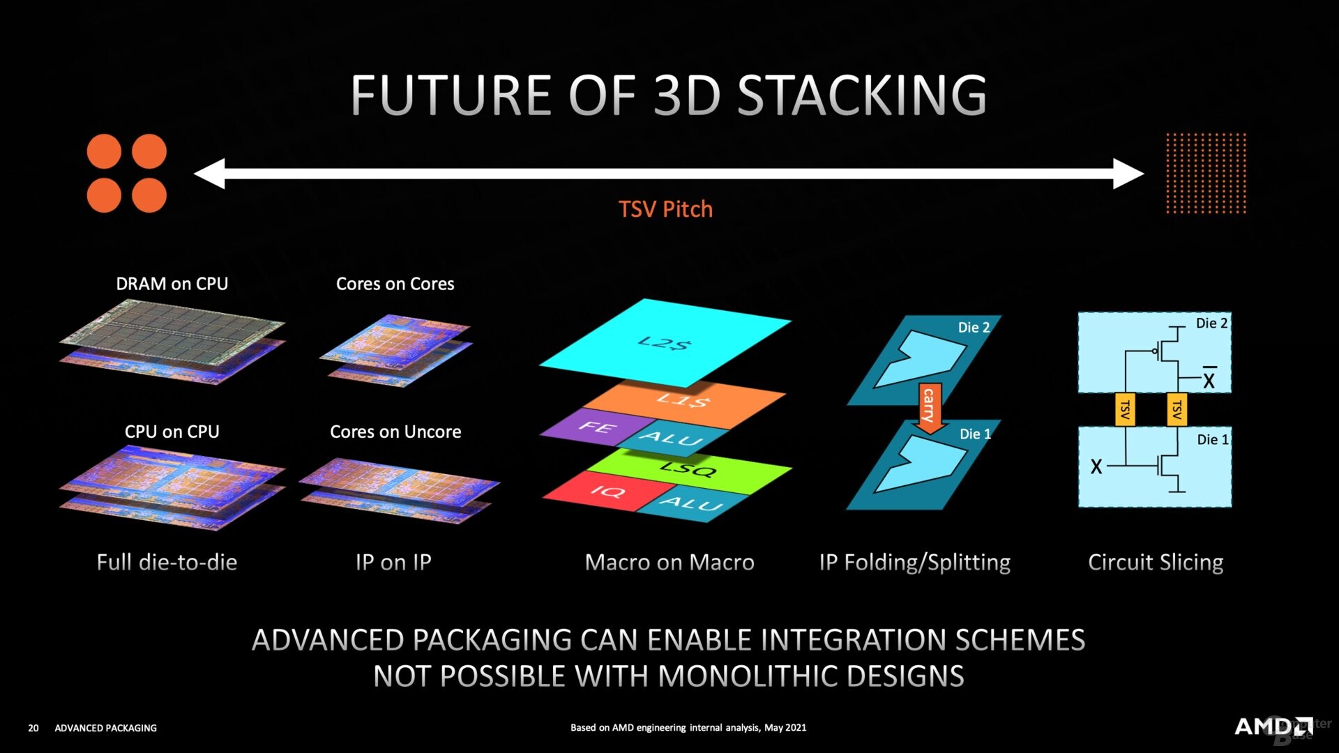
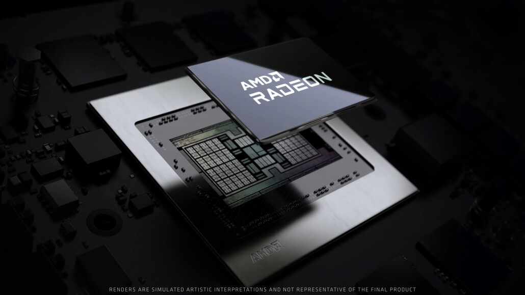
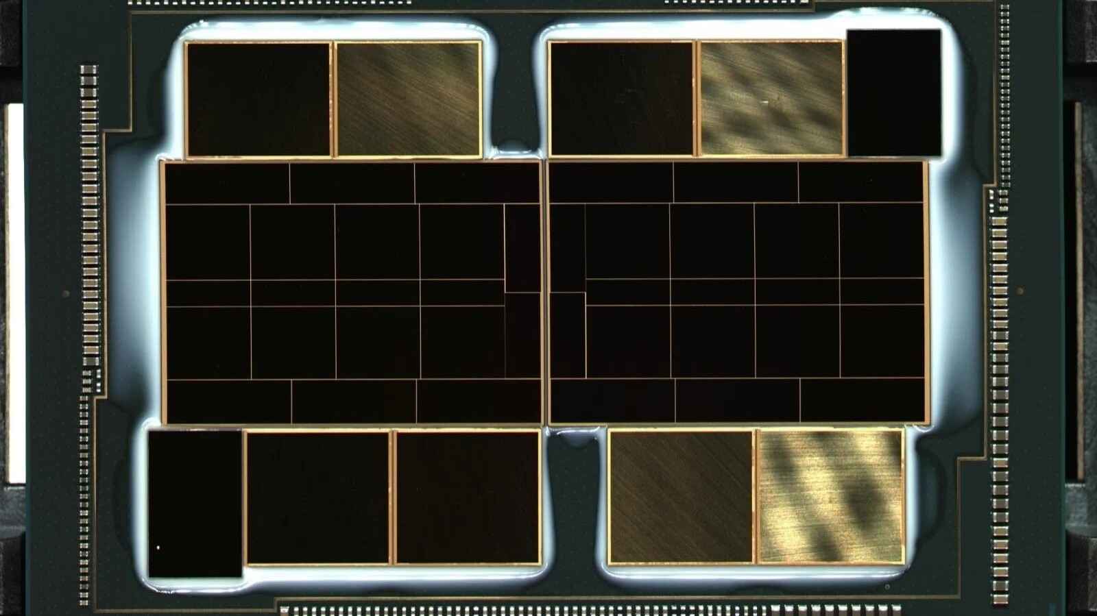
AMD via its official YouTube has shared a video that goes into slightly more detail on their usage of V-Cache on the upcoming Zen 3+ CPUs. Firstly demoed to the public on AMD's Computex 2021 event, the 3D V-Cache leverages TSMC's SoIC stacking technology, which enables silicon developments along the Z axis, instead of the more usual footprint increase along the X axis. The added 3D V-Cache, which was shown in Computex as being deployed in a prototype Ryzen 9 5900X 12-core CPU, adds 64 MB of L3 cache to each CCX (the up-to-eight-cores core complex on AMD's latest Zen design), basically tripling the amount of L3 cache available for the CPU. This, in turn, was shown to increase FPS in games quite substantially (somewhere around 15%), as games in particular are sensitive to this type of CPU resources.

The added information explains that there is no usage of microbumps - instead, there is a perfect alignment between the bottom layer (with the CCX) and the top layer (the L3 cache) which enables the bonding process to occur naturally via the TSVs (Through Silicon Vias) already present in the silicon, in a zero-gap manner, between both halves of the CPU-cache sandwich. To enable this, AMD flipped the CCX upside down (the core complex now faces the bottom of the chip, instead of the top), shaved 95% of the silicon on top of the upside-down core complexes, and then attaches the 3D V-Cache chips on top of this formation. This also has the added bonus of decreasing the distance between the L3 cache and the CCX (the distance between both in the Z axis is around 1,000 times smaller than if the L3 cache was deployed in the classical X axis), which decreases power consumption, temperatures, and latency, allowing for further increases to system performance. Look after the break for the full video.

TSMC 4nm Production Hit By... A Full Quarter Advance?

Here's something that has been sorely missing from tech news: good news. It seems that TSMC's development on the 4 nm manufacturing process is running better than anticipated by the company itself, which has prompted for a full quarter advancement for the test production on TSMC's next miniaturization level. Previously scheduled for test production starting on 4Q 2021, TSMC has announced that it has now moved test production to 3Q 2021.

This could mean an equivalent - or perhaps even better - reduction in volume production and time-to-market, but it's anyone's guess at this point. As notably difficult and onerous as semiconductor development is, problems are more likely to appear than not. 4 nm is expected to bring respectable improvements to the PPA equation for semiconductors over 5 nm - however, TSMC still hasn't disclosed expected gains.

AMD Ryzen 8000 Series Processors Based on Zen 5 Architecture Reportedly Codenamed "Granite Ridge"

Today, we have talked about AMD's upcoming Raphael lineup of processors in the article you can find here. However, it seems like the number of leaks on AMD's plans just keeps getting greater. Thanks to the "itacg" on Weibo, we have learned that AMD's Ryzen 8000 desktop series of processors are reportedly codenamed as Granite Ridge. This new codename denotes the Zen 5 based processors, manufactured on TSMC's 3 nm (N3) node. Another piece of information is that AMD's Ryzen 8000 series APUs are allegedly called Strix Point, and they also use the 3 nm technology, along with a combination of Zen 5 and Zen 4 core design IPs. We are not sure how this exactly works out, so we have to wait to find out more.

Second TSMC Fab Worker Detected with COVID-19, Chip Shortages on the Anvil?

Taiwan's most valuable company, and chipmaker of the world, TSMC, confirmed that at least two of its fab workers have been diagnosed with COVID-19, but maintains that it doesn't affect operations at the plants. Most regions around world, including Taiwan, are bracing for successive waves of the disease, and a spread of COVID at TSMC could spell big trouble for the tech-giants dependent on the company for contract-manufacturing of their cutting-edge logic chips. Taiwan has been mostly spared from the Corona epidemic, but is now experiencing its largest wave of COVID-19 infections, with its medical infrastructure under strain. The latest outbreak has the potential to throw operations at TSMC off gear, affecting the supply chains of tens of billions of Dollars worth devices and vehicles around the world.

TSMC maintains an internal epidemic prevention committee, which has conducted contact-tracing of the the two employees, and discovered 10 contacts. Some of these have been sent to home-isolation, while others are closely monitoring themselves for symptoms. TSMC pledged that it will monitor the health of its employees on a daily basis. It has also completed the disinfection of the affected employees' workplace, and public areas visited by them. It once again emphasized that the incident will not affect company operations.

Cadence Announces New Low-Power IP for PCI Express 5.0 Specification on TSMC N5 Process

Cadence Design Systems, Inc. (Nasdaq: CDNS) today announced immediate availability of Cadence IP supporting the PCI Express (PCIe ) 5.0 specification on TSMC N5 process technology. The next follow-on version on TSMC N3 process technology is expected to be taped out in early 2022. Collaboration with major customers is ongoing for N5 SoC designs targeting hyperscale computing and networking applications. The Cadence IP for PCIe 5.0 technology consists of a PHY, companion controller and Verification IP (VIP) targeted at SoC designs for very high-bandwidth hyperscale computing, networking and storage applications. With Cadence's PHY and Controller Subsystem for PCIe 5.0 architecture, customers can design extremely power-efficient SoCs with accelerated time to market.

The Cadence IP for PCIe 5.0 architecture offers a highly power-efficient implementation of the standard, with several evaluations from leading customers indicating it provides industry best-in-class power at the maximum data transfer rate of 32GT/s and worst-case insertion loss. Leveraging Cadence's existing N7/N6 silicon validated offering, the N5 design provides a full 512GT/s (gigatransfers per second) power-optimized solution across the full range of operating conditions with a single clock lane.

TSMC Claims Breakthrough on 1nm Chip Production

TSMC in collaboration with the National Taiwan University (NTU) and the Massachusetts Institute of Technology (MIT) have made a significant breakthrough in the development of 1-nanometer chips. The joint announcement comes after IBM earlier this month published news of their 2-nanometer chip development. The researchers found that the use of semi-metal bismuth (Bi) as contact electrodes for the 2D matrix can greatly reduce resistance and increase current. This discovery was first made by the MIT team before then being further refined by TSMC and NTU which will increase energy efficiency and performance in future processors. The 1-nanometer node won't be deployed for several years with TSMC planning to start 3-nanometer production in H2 2022.
Return to Keyword Browsing
Apr 25th, 2024 06:57 EDT change timezone

New Forum Posts

Popular Reviews

Controversial News Posts