News Posts matching #TSMC

Return to Keyword Browsing

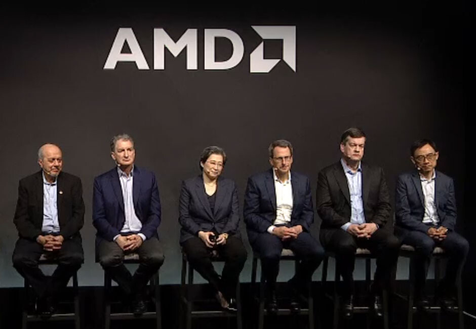
Huawei's Loss AMD's Gain, TSMC Develops Special 5nm Node

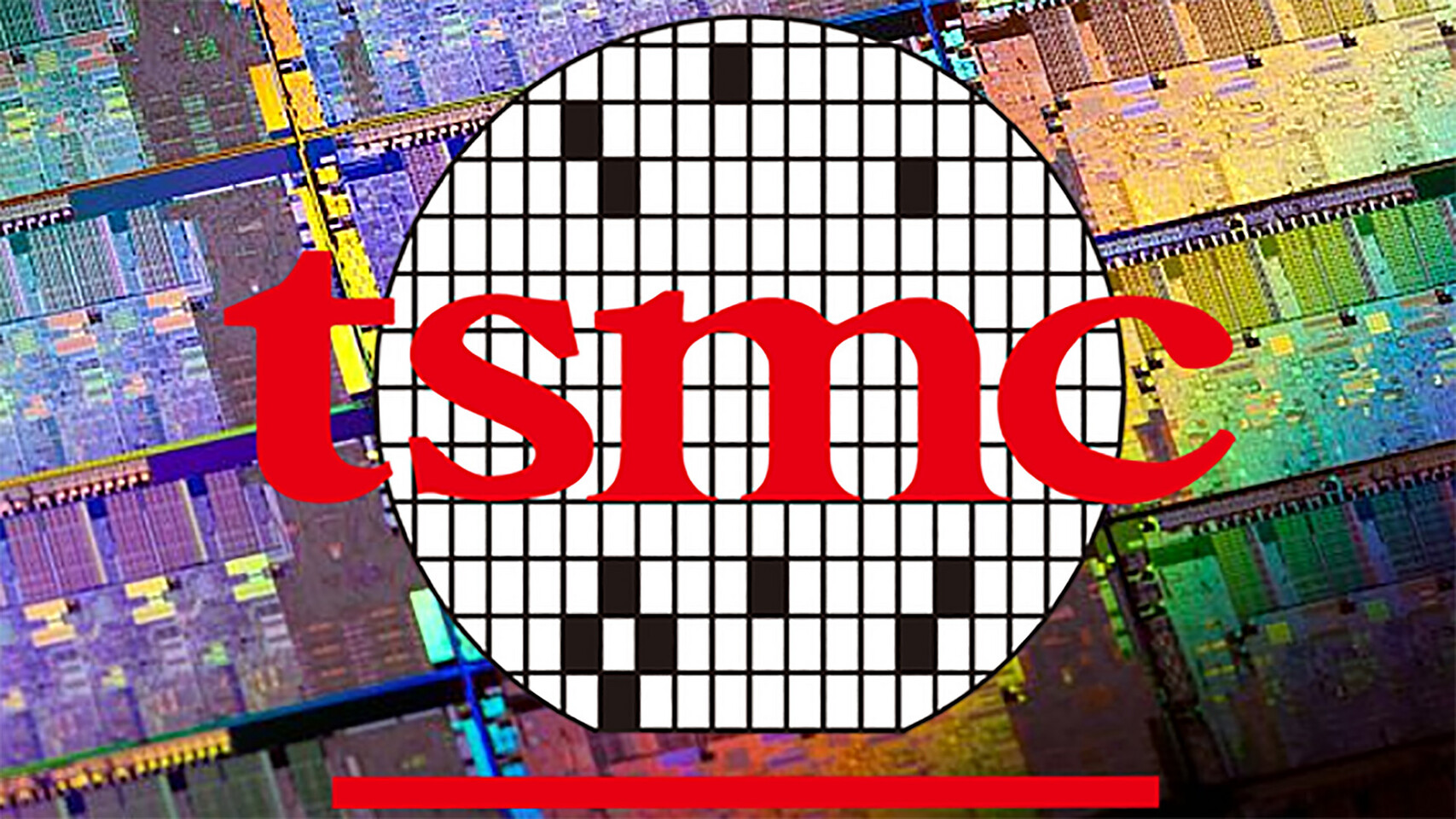
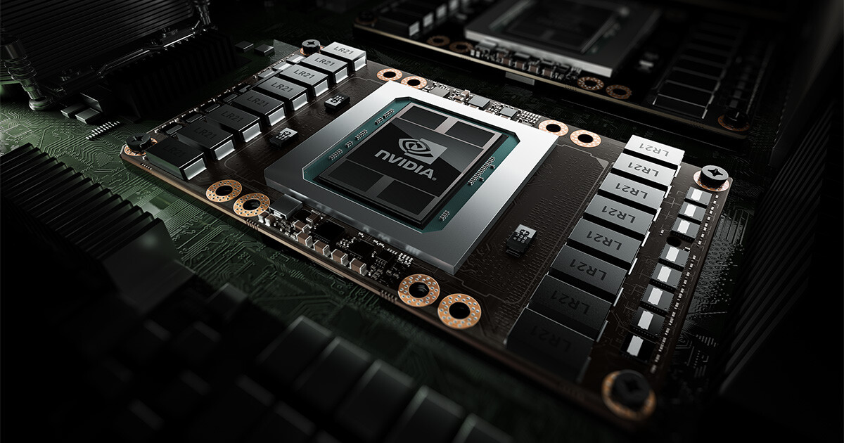
With Mainland Chinese tech giant Huawei being effectively cut off from contracting Taiwanese TSMC to manufacture its next-generation HiSilicon 5G mobile SoCs, and NVIDIA switching to Samsung for its next-generation GPUs, TSMC is looking to hold on to large high-volume customers besides Apple and Qualcomm, so as to not let them dictate pricing. AMD is at the receiving end of the newfound affection, with the semiconductor firm reportedly developing a new refinement of its 5 nm node specially for AMD, possibly to make Sunnyvale lock in on TSMC for its future chip architectures. A ChainNews report decoded by @chiakokhua sheds light on this development.

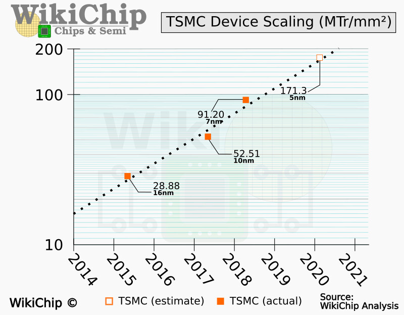
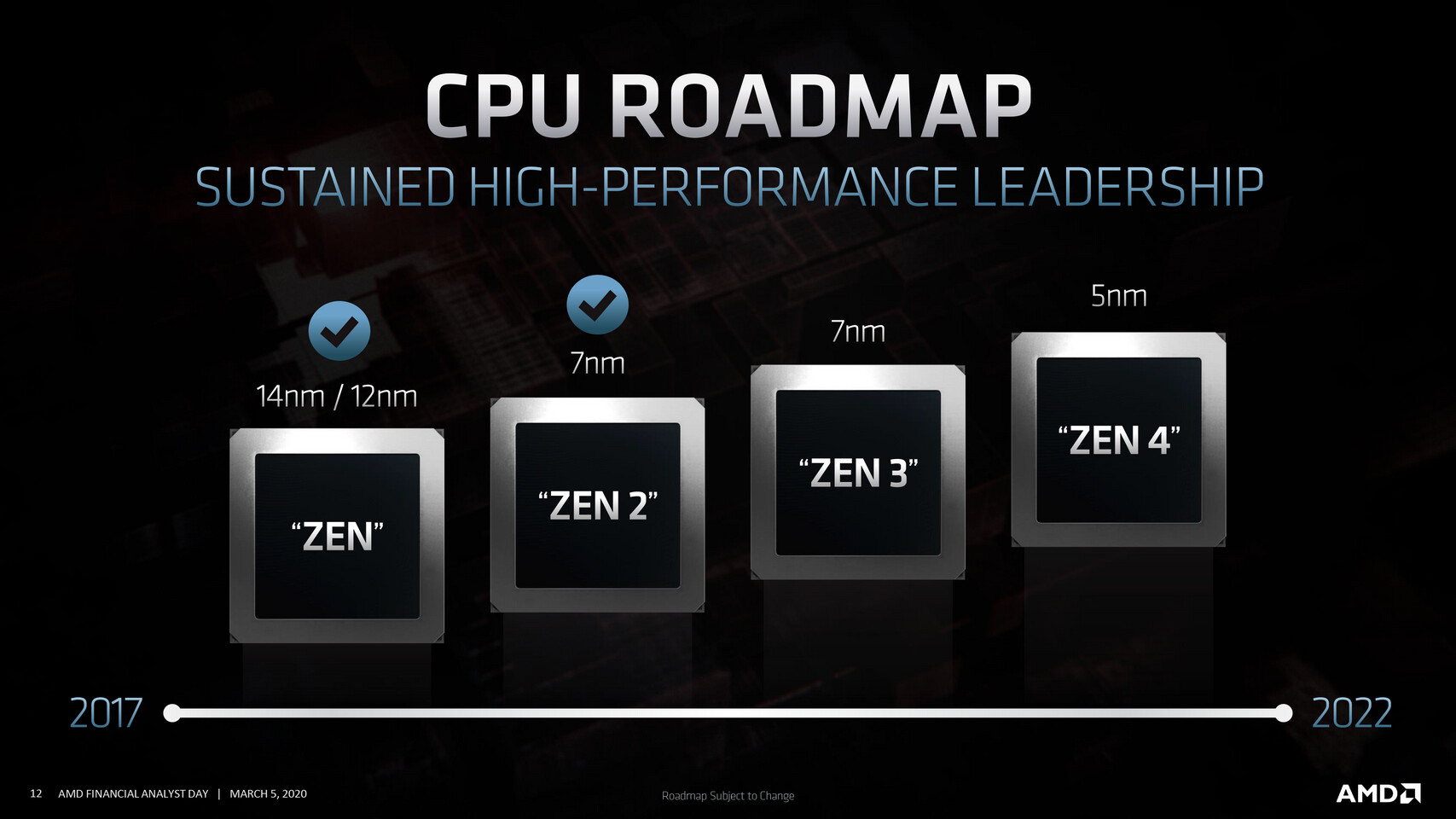
AMD is developing its "Zen 4" CPU microarchitecture for a 5 nm-class silicon fabrication node, although the company doesn't appear to have zeroed in on a node for its RDNA3 graphics architecture and CDNA2 scalar compute architecture. In its recent public reveal of the two, AMD chose not to specify the foundry node for the two, which come out roughly around the same time as "Zen 4." It wouldn't be far fetched to predict that AMD and TSMC were waiting on certainty for the new 5 nm-class node's development. There are no technical details of this new node. AMD's demand for TSMC is expected to be at least 20,000 12-inch wafers per month.

Apple's A12Z SoC Features the Same A12X Silicon

With an introduction of new iPad Pro tablets, Apple has brought another new silicon to its offerings in the form of A12Z SoC. Following the previous king in tablet space, the A12X SoC, Apple has decided to update its silicon and now there is another, more advanced stepping in form of an A12Z SoC. Thanks to the report from TechInsights, their analysis has shown that the new SoC used in Apple's devices is pretty much the same compared to the A12X SoC of last year, except the GPU used. Namely, the configuration of A12X is translated into the A12Z - there are four Apple Vortex and four Apple Tempest cores for the CPU. There is a 128-bit memory bus designed for LPDDR4X memory, the same as the A12X.

What is different, however, is the GPU cluster configuration. In A12X there was a cluster filled with 7 working and one disabled A12-gen GPU core. In A12Z SoC all of the 8 GPUs present are enabled and working, and they are also of the same A12 generation. The new SoC is even built using the same N7 7 nm manufacturing process from TSMC. While we don't know the silicon stepping revision of the A12Z, there aren't any new features besides the additional GPU core.
Apple A12Z Bionic

Huawei Moves 14 nm Silicon Orders from TSMC to SMIC

Huawei's subsidiary, HiSilicon, which designs the processors used in Huawei's smartphones and telecommunications equipment, has reportedly moved its silicon orders from Taiwan Semiconductor Manufacturing Company (TSMC) to Semiconductor Manufacturing International Corporation (SMIC), according to DigiTimes. Why Huawei decided to do is move all of the 14 nm orders from Taiwanese foundry to China's largest silicon manufacturing fab, is to give itself peace of mind if the plan of the US Government goes through to stop TSMC from supplying Huawei. At least for the mid-tier chips built using 14 nm node, Huawei would gain some peace as a Chinese fab is a safer choice given the current political situation.

When it comes to the high-end SoCs built on 7 nm, and 5 nm in the future, it is is still uncertain how will Huawei behave in this situation, meaning that if US cuts off TSMC's supply to Huawei, they will be forced to use SMIC's 7 nm-class N+1 node instead of anything from TSMC. Another option would be Samsung, but it is a question will Huawei put itself in risk to be dependant on another foreign company. The lack of 14 nm orders from Huawei will not be reflecting much on TSMC, because whenever someone decides to cut orders, another company takes up the manufacturing capactiy. For example, when Huawei cut its 5 nm orders, Apple absorbed by ordering more capacity. When Huawei also cut 7 nm orders, AMD and other big customers decided to order more, making the situation feel like there is a real fight for TSMC's capacity.
Silicon Wafer

TSMC Sees Higher Demand for CoWoS Packaging

TSMC, Taiwan's flagship manufacturer of silicon, has seen a substantial increase in demand for Chip-on-Wafer-on-Substrate (CoWoS) packaging technology, according to the report from DigiTimes. CoWoS is a multi-chip packaging technology that gives an option to build silicon like LEGO, allowing for dies to be placed side by side on interposer that is providing high interconnect density and performance. You can see more about CoWoS in detail here. Some of the examples of CoWoS are NVIDIA's P100 and V100 dies that integrate logic (computing elements), and memory (in the form of HBM) on a single die.

Recently, TSMC updated its CoWoS technology, where this new second-generation parts could scale far larger than the first-generation implementation - up to 1700 squared millimeters of die space, allowing for some very creative solutions to be implemented. This may be the reason that the demand in Q2 has risen so substantially and that TSMC's production lines are now running at full capacity, trying to meet the demand for this packaging technology.
TSMC CoWoS NVIDIA V100

AMD 4th Gen Ryzen Desktop Processors to Launch Around September 2020

AMD's 4th generation Ryzen desktop processors are expected to launch around September 2020, sources in the motherboard industry tell DigiTimes. Codenamed "Vermeer," successor to "Matisse," these processors will be socket AM4 multi-chip modules of up to two CPU complex dies based on the "Zen 3" microarchitecture, combined with an I/O controller die. The "Zen 3" chiplets are expected to be fabricated on a newer 7 nm-class process by TSMC, either N7P or N7+. The biggest design change with "Zen 3" is the doing away of CCX arrangement of CPU cores, with each chiplet holding a common block of cores sharing a last-level cache. This, along with clock speed headroom gains from the new node are expected to yield generational price-performance increases.

The "Zen 2" based 8-core "Renoir" die is also expected to make its socket AM4 debut within 2020, succeeding the "Picasso" based quad-core Ryzen 3000-series APUs. This is a particularly important product for AMD, as it is expected to compete with Intel's 10th generation Core i5 6-core/12-thread processors in terms of pricing, while offering more cores (8-core/16-thread) and a faster iGPU. The 4th gen Ryzen socket AM4 processor lineup will launch alongside AMD's 600-series motherboard chipset, with forwards- and backwards-compatibility (i.e., "Vermeer" and "Renoir" working with older chipsets, and older AM4 processors working on 600-series chipset motherboards). AMD was originally expected to unveil these processors at the 2020 Computex trade-show in June, but Computex itself is rescheduled to late-September.

SMIC 7nm-class N+1 Foundry Node Going Live by Q4-2020

China's state-backed SMIC (Semiconductor Manufacturing International Corporation) has set an ambitious target of Q4-2020 for its 7 nanometer-class N+1 foundry node to go live, achieving "small scale production," according to a cnTechPost report. The company has a lot of weight on its shoulders as geopolitical hostility between the U.S. and China threatens to derail the country's plans to dominate 5G technology markets around the world. The SMIC N+1 node is designed to improve performance by 20%, reduce chip power consumption by 57%, reduce logic area by 63%, and reduce SoC area by 55%, in comparison to the SMIC's 14 nm FinFET node, Chinese press reports citing a statement from SMIC's co-CEO Dr. Liang Mengsong.

Dr. Liang confirmed that the N+1 7 nm node and its immediate successor will not use EUV lithography. N+1 will receive a refinement in the form of N+2, with modest chip power consumption improvement goals compared to N+1. This is similar to SMIC's 12 nm FinFET node being a refinement of its 14 nm FinFET node. Later down its lifecycle, once the company has got a handle of its EUV lithography equipment, N+2 could receive various photomasks, including a switch to EUV at scale.

U.S. Government Tightens Screws on Huawei's Global Chip Supply from TSMC

The U.S. government announced advanced measures that make it harder for foreign companies, such as Taiwan's TSMC, to supply chips to Chinese telecom hardware giant Huawei. Foreign companies that use American chipmaking equipment, are required to obtain a license from the U.S. before supplying certain chips to Huawei. Sources comment that the new rule was tailor-made to curb TSMC fabricating smartphone SoCs for Huawei's HiSilicon subsidiary.

Mainland Chinese semiconductor companies are still behind Samsung and TSMC in 7 nm-class fab technologies, forcing HiSilicon to source from the latter. 7 nm fabrication is a key requirement for SoCs and modem chips capable of 5G. The high data transceiving rates of 5G requires a certain amount of compute power that can fit into smartphone-level power-envelopes only with the help of 7 nm, at least for premium smartphone form-factors. Same applies to 5G infrastructure equipment. This is hence perceived as a means for the U.S. to clamp brakes on Huawei's plans of playing a big role in 5G tech rollouts around the world, buying western 5G tech suppliers such as Nokia time to catch up. Huawei has been a flashpoint for a bitter political spat between the U.S. and China, with the Chinese press even threatening that the matter could hamper medical supplies to the U.S. to fight the COVID-19 pandemic.

TSMC N5P 5nm Node Offers 84-87% Transistor Density Gain Over Current 7nm Node

A WikiChip analysis of TSMC's next-generation 5 nanometer N5P silicon fabrication node estimates a massive 84-87% increase in transistor densities on offer compared to the company's first commercial 7 nm-class node, the N7 (7 nm DUV). The report estimates an 87% transistor-density increase, even though TSMC's own figure is slightly modest, at 84%. TSMC N5P node is expected to commence production later this year. Its precursor, TSMC N5, began risk production earlier this year, with production on the node commencing in April or May, unless derailed by the COVID-19 pandemic. The N5P node provides transistor densities of an estimated 171.3 million transistors per mm² die area, compared to 91.2 mTr/mm² of N7. Apple is expected to be the node's biggest customer in 2020, with the company building its A14-series SoC on it.

TSMC to Kickstart 5 nm Volume Production in April, Production Capacity Already Fully Booked

TSMC will be doing good on their previous expectations for a H2 2020 ramp-up for high volume production (HVM) on their 5 nm manufacturing process. The new 5 nm fabrication process is an Extreme Ultraviolet lithography (EUV) one, with up to 14 layers being etchable onto the silicon wafers, as opposed to five and six, respectively, for TSMC's N7+ and N6 processes.

Volume production will start with Apple's A14 SoC, meant to be driving next-generation iPhones that should hit shelves by September this year (should the COVID-19 pandemic let it be so). Apple is using two thirds of TSMC's capacity for 5 nm as is with this SoC; it's currently unclear which client (or clients) are getting the leftover one third capacity. TSMC announced back in December that they were seeing yields upwards of 80% in 5 nm EUV fabrication, so now it's "just" a matter of monetizing the process until their 3 nm iteration comes online, expectedly, in 2022.

Xilinx Announces World's Highest Bandwidth, Highest Compute Density Adaptable Platform for Network and Cloud Acceleration

Xilinx, Inc. today announced Versal Premium, the third series in the Versal ACAP portfolio. The Versal Premium series features highly integrated, networked and power-optimized cores and the industry's highest bandwidth and compute density on an adaptable platform. Versal Premium is designed for the highest bandwidth networks operating in thermally and spatially constrained environments, as well as for cloud providers who need scalable, adaptable application acceleration.

Versal is the industry's first adaptive compute acceleration platform (ACAP), a revolutionary new category of heterogeneous compute devices with capabilities that far exceed those of conventional silicon architectures. Developed on TSMC's 7-nanometer process technology, Versal Premium combines software programmability with dynamically configurable hardware acceleration and pre-engineered connectivity and security features to enable a faster time-to-market. The Versal Premium series delivers up to 3X higher throughput compared to current generation FPGAs, with built-in Ethernet, Interlaken, and cryptographic engines that enable fast and secure networks. The series doubles the compute density of currently deployed mainstream FPGAs and provides the adaptability to keep pace with increasingly diverse and evolving cloud and networking workloads.
Xilinx Versal ACAP FPGA

Intel Courts TSMC 6nm and 3nm Nodes for Future Xe GPU Generations

Intel is rumored to be aligning its future-generation Xe GPU development with TSMC's node development cycle, with the company reportedly negotiating with the Taiwanese foundry for 6 nm and 3 nm allocation for its large Xe GPUs. Intel's first Xe discrete GPUs for the market, however, are reportedly built on the company's own 10 nm+ silicon fabrication process.

While Intel's fascination with TSMC 3 nm is understandable, seeking out TSMC's 6 nm node raises eyebrows. Internally referred to as "N6," the 6 nm silicon fabrication node at TSMC is expected to go live either towards the end of 2020 or early 2021, which is when Intel's 10 nm+ node is expected to pick up volume production, beginning with the company's "Tiger Lake" processors. Perhaps a decision has been made internally to ensure that Xe doesn't eat too much into Intel's own foundry capacities meant for processor manufacturing, and to instead outsource Xe manufacturing to third-party foundries like TSMC and Samsung eventually. Way back in April 2019 it was rumored that Intel was evaluating Samsung as a foundry partner for Xe.

AMD Sheds Light on the Missing "+" in "7nm" for Zen 3 and RDNA2 in its Latest Presentation

AMD at its Financial Analyst Day 2020 presentation made a major clarification about its silicon fabrication process. It was previously believed that the company's upcoming "Zen 3" CPU microarchitecture and RDNA2 graphics architectures were based on TSMC's N7+ (7 nm EUV) silicon fabrication process because AMD would mark the two as "7 nm+" in its marketing slides. Throughout its Financial Analyst Day presentation, however, AMD avoided using that marker, and resorted to an amorphous "7 nm" marker, prompting one of the financial analysts to seek a clarification. At the time, AMD responded that they were aligning their marketing with that of TSMC, and hence chose to use "7 nm" in its new slides.

It turns out that the next step to TSMC N7, the company's current-generation 7 nm DUV silicon fabrication node, isn't N7+ (7 nm EUV), but rather it has a nodelet along the way, which the foundry refers to as N7P. This is a generational refinement of N7, but does not use EUV lithography, which means it may not offer the 15-20 percent gains in transistor densities offered by N7+ over N7. AMD clarified that "7 nm+" in its past presentations did not intend to signify N7+, and that the "+" merely denoted an improvement over N7. At the same time, it won't specify whether "Zen 3" and RDNA2 are based on N7P or N7+, so the company doesn't rule out N7+, either. We'll probably learn more as we near the late-2020 launch of "Zen 3" as EPYC "Milan."
AMD CPU Roadmap Zen 3 Zen 4 AMD CPU Roadmap Zen 2 Zen 3

AMD Financial Analyst Day 2020 Live Blog

AMD Financial Analyst Day presents an opportunity for AMD to talk straight with the finance industry about the company's current financial health, and a taste of what's to come. Guidance and product teasers made during this time are usually very accurate due to the nature of the audience. In this live blog, we will post information from the Financial Analyst Day 2020 as it unfolds.
20:59 UTC: The event has started as of 1 PM PST. CEO Dr Lisa Su takes stage.

Ampere Computing Uncovers 80 Core "Cloud-Native" Arm Processor

Ampere Computing, a startup focusing on making HPC and processors from cloud applications based on Arm Instruction Set Architecture, today announced the release of a first 80 core "cloud-native" processor based on the Arm ISA. The new Ampere Altra CPU is the company's first 80 core CPU meant for hyper scalers like Amazon AWS, Microsoft Azure, and Google Cloud. Being built on TSMC's 7 nm semiconductor manufacturing process, the Altra is a CPU that is utilizing a monolithic die to achieve maximum performance. Using Arm's v8.2+ instruction set, the CPU is using the Neoverse N1 platform as its core, to be ready for any data center workload needed. It also borrows a few security features from v8.3 and v8.5, namely the hardware mitigations of speculative attacks.

When it comes to the core itself, the CPU is running at 3.0 GHz frequency and has some very interesting specifications. The design of the core is such that it is 4-wide superscalar Out of Order Execution (OoOE), which Ampere refers to as "aggressive" meaning that there is a lot of data throughput going on. The cache levels are structured in a way that there is 64 KB of L1D and L1I cache per core, along with 1 MB of L2 cache per core as well. For system-level cache, there is 32 MB of L3 available to the SoC. All of the caches have Error-correcting code (ECC) built-in, giving the CPU a much-needed feature. There are two 128-bit wide Single Instruction Multiple Data (SIMD) units, which are there to do parallel processing if needed. There is no mention if they implement Arm's Scalable Vector Extensions (SVE) or not.

TSMC and Broadcom Enhance the CoWoS Platform with World's First 2X Reticle Size Interposer

TSMC today announced it has collaborated with Broadcom on enhancing the Chip-on-Wafer-on-Substrate (CoWoS ) platform to support the industry's first and largest 2X reticle size interposer. With an area of approximately 1,700mm2, this next generation CoWoS interposer technology significantly boosts computing power for advanced HPC systems by supporting more SoCs as well as being ready to support TSMC's next-generation five-nanometer (N5) process technology.

This new generation CoWoS technology can accommodate multiple logic system-on-chip (SoC) dies, and up to 6 cubes of high-bandwidth memory (HBM), offering as much as 96 GB of memory. It also provides bandwidth of up to 2.7 terabytes per second, 2.7 times faster than TSMC's previously offered CoWoS solution in 2016. With higher memory capacity and bandwidth, this CoWoS solution is well-suited for memory-intensive workloads such as deep learning, as well as workloads for 5G networking, power-efficient datacenters, and more. In addition to offering additional area to increase compute, I/O, and HBM integration, this enhanced CoWoS technology provides greater design flexibility and yield for complex ASIC designs in advanced process nodes.

TSMC to Hire 4000 new Staff for Next-Generation Semiconductor Node Development

TSMC is set to hire about 4000 new staff members to gain a workforce for its development of next-generation semiconductor manufacturing nodes. The goal of the company is to gather talent so it can develop the world's leading semiconductor nodes, like 3 nm and below. With 15 billion USD planned for R&D purposes alone this year, TSMC is investing a big part of its capital back into development on new and improved technology. Markets such as 5G and High-Performance Computing are leading the charge and require smaller, faster, and more efficient semiconductor nodes, which TSMC plans to deliver. To gather talent, TSMC started job listing using recruitment website TaiwanJobs and started campaigns on university campuses to attract grad students.

Apple to Launch Arm-Powered MacBook in the next 18 Months

Apple is currently designing a custom series of CPUs, for its Macbook laptop lineup, based on the Arm Instruction Set Architecture. Having designed some of the most powerful mobile processors that are inside the iPhone series of devices, Apple is preparing to make a jump to an even more powerful device lineup by bringing custom CPUs for MacBook. Tired of the speed by which Intel replaces and upgrades its Core lineup of CPUs, Apple decided to take the matter in its own hands and rumors about the switch to a custom solution have been going on for a while. However, we now have some information about when to expect the first wave of Arm-powered Macs.

According to the analyst Ming-Chi Kuo, who is a well-known insider in the Apple industry, we can expect the first wave of the Arm-powered Macbook in the next 18 months, precisely in the first half of 2021. Supposedly, the first chips for these new Macs are going to be manufactured on a 5 nm manufacturing process, possibly over at TSMC since Apple had a long-lasting history of manufacturing its chips at TSMC foundries. In the meantime, we can expect to see Apple providing developers with tools to transition their x86-64 software to the new Arm ISA. Without a software ecosystem, the hardware platform is essentially worthless. And Apple knows this. We will see how they plan to play it and will report as soon as there is more information.

Ruijie RG-CT7800 Mini-PC Among First Zhaoxin KaiXian Designs, Tip of China's 3-5-2 Spear

With a 2.4-liter volume, a conventional black plastic body, and essential connectivity, the Ruijie RG-CT7800 may come across as a run-of-the-mill mini-PCs for small businesses or those who do precious little offline, except what's under the hood. This humble compact desktop is among the first design wins of China's ambitious effort at having an x86 processor built entirely on Chinese soil, the Zhaoxin KaiXian. This processor is making its way to products, and was recently pictured on an embedded motherboard. The KaiXian, along with the notebooks, motherboards, micro-servers, and mini-PCs that implement it, form the tip of China's 3-5-2 policy, an ambitious plan to rid all state- and state-owned institutions of "foreign hardware."

The numerals in "3-5-2" are supposed to correspond to foreign hardware replacement targets set by the country's Central Government - 30% by the end of 2020, an additional 50% by the end of 2021, and the remaining 20% by the end of 2022. To support this plan, the Chinese electronics industry, flush with state investment, has indigenized several key components of the modern PC, including DRAM, NAND flash, and now CPU. The country already dominates the global electronic components market. The RG-CT7800 implements The KaiXian KX-U6780A SoC that sports eight x64 CPU cores running at 2.70 GHz. Interestingly, the chip is manufactured on TSMC's 16 nm FinFET node (a de facto "foreign" source, but one that's de jure China from Beijing's perspective). Ruijie is equipping the RG-CT7800 with 8 GB of DDR4 memory, and 256 GB of SSD-based storage. One can make out industry-standard USB, Ethernet, 3.5 mm audio jacks, etc., from the pictures. The box will be compatible with UOS and NeoKylin (Linux distros built under scrutiny of the Chinese Government). With state institutions being on the clock to implement their 3-5-2 targets, it's possible that the first volumes of RG-CT7800 will be sold exclusively to state customers.

US Government Could Stop Chip Shipments from TSMC to Huawei

US Government, precisely the Trump administration, is considering placing a ban on chip export from TSMC to Huawei. With Huawei being in the middle between the US and China fight for global technology dominance, the Trump administration is seeking to limit the progress of foreign forces trying to match or beat US technology. There were previous efforts by the US government to influence Huawei's fate, with them claiming that Huawei 5G equipment is capable of supplying China with intelligence, meaning that China tries to spy on US citizens. While those claims were later disregarded by Huawei, the Trump administration managed to do some damage to the face of the company.

The TSMC representative who spoke to Reuters about the potential ban said that the company (TSMC) does not answer hypothetical questions and that they don't talk about their customers. To achieve more control over the China semiconductor manufacturing, the US government plans to place a licensing model on all of their US-made semiconductor equipment, meaning that all the production lines are possibly in danger if the US doesn't approve shipments of their machines to other countries.

VIA CenTaur CHA NCORE AI CPU Pictured, a Socketed LGA Package

VIA's CenTaur division sprung an unexpected surprise in the CPU industry with its new CHA x86-64 microarchitecture and an on-die NCORE AI co-processor. This would be the first globally-targeted x86 processor launch by a company other than Intel and AMD in close to 7 years, and VIA's first socketed processor in over 15 years. SemiAccurate scored a look at mock-up of the CenTaur CHA NCORE 8-core processor and it turns out that the chip is indeed socketed.

Pictured below, the processor is a flip-chip LGA. We deduce it is socketed looking at its alignment notches and traces for ancillaries on the reverse-side (something BGAs tend to lack). On the other hand, the "contact points" of the package appear to cast shadows, and resemble balls on a BGA package. Topside, we see an integrated heatspreader (IHS), and underneath is a single square die. CenTaur built the CHA NCORE on TSMC's 16 nm FinFET process. The package appears to have quite a high pin-count for a die this size, but that's probably because of its HEDT-rivaling I/O, which includes a quad-channel DDR4 memory interface and 44 PCI-Express gen 3.0 lanes.

TSMC Sets Aside Almost 7 Billion Dollars for Fab Expansion

TSMC is working hard to ensure its number one spot in the semiconductor manufacturing industry, and it has the funds to back it up. Yesterday TSMC's Board of Directors approved the company budget for another semiconductor fab expansion. With a budget totaling 6.74 billion US dollars allocated, TSMC has "Approved capital appropriations of approximately US$6,742.1 million (approximately NT$200.9 billion) for purposes including: 1) Fab construction, and installation of fab facility systems; 2) Installation and upgrade of advanced technology capacity; 3) Installation of specialty technology capacity; 4) Installation of advanced packaging capacity; 5) Second quarter 2020 R&D capital investments and sustaining capital expenditures."

Zhaoxin KaiXian x86 Processor Now Commercially Available to the DIY Channel

Zhaoxin is a brand that makes multi-core 64-bit x86 processors primarily for use in Chinese state IT infrastructure. It's part of the Chinese Government's ambitious plan to make its IT hardware completely indigenous. Zhaoxin's x86-64 CPU cores are co-developed by licensee VIA, specifically its CenTaur subsidiary that's making NCORE AI-enabled x86 processors. The company's KaiXian KX-6780A processor is now commercially available in China to the DIY market in the form of motherboards with embedded processors.

The KaiXian KX-6780A features an 8-core/8-thread x86-64 CPU clocked up to 2.70 GHz, 8 MB of last-level cache, a dual-channel DDR4-3200 integrated memory controller, a PCI-Express gen 3.0 root-complex, and an iGPU possibly designed by VIA's S3 Graphics division, which supports basic display and DirectX 11.1 readiness. The CPU features modern ISA, with instruction sets that include AVX, AES-NI, SHA-NI, and VT-x comparable virtualization extensions. The chip has been fabricated on TSMC 16 nm FinFET process.

AMD to Debut 2nd Gen RDNA Architecture in 2020

AMD CEO Dr Lisa Su, in her Q4-2019 and FY-2019 earnings call, confirmed that the company debut its second-generation RDNA graphics architecture in 2020. "In 2019 we launched our new architecture in GPUs, it's the RDNA architecture, and that was the Navi-based products. You should expect those will be refreshed in 2020, and we will have our new next-generation RDNA architecture that will be part our 2020 lineup."

Second-gen RDNA, or RDNA2, is expected to leverage the new 7 nm+ (EUV) silicon fabrication process at TSMC, to dial up transistor-counts, clock-speeds, and performance. Among the two anticipated feature additions are VRS (variable rate shading) and possibly ray-tracing. The fabled "big Navi" silicon, a GPU larger than "Navi 10," is also on the cards, according to an earlier statement by Dr Su. More details about these upcoming graphics cards are expected to be put out in March, at the 2020 AMD Investor Day conference.

Europe Readies its First Prototype of Custom HPC Processor

European Processor Initiative (EPI) is a Europe's project to kickstart a homegrown development of custom processors tailored towards different usage models that the European Union might need. The first task of EPI is to create a custom processor for high-performance computing applications like machine learning, and the chip prototypes are already on their way. The EPI chairman of the board Jean-Marc Denis recently spoke to the Next Platform and confirmed some information regarding the processor design goals and the timeframe of launch.

Supposed to be manufactured on TSMC's 6 nm EUV (TSMC N6 EUV) technology, the EPI processor will tape-out at the end of 2020 or the beginning of 2021, and it is going to be heterogeneous. That means that on its 2.5D die, many different IPs will be present. The processor will use a custom ARM CPU, based on a "Zeus" iteration of Neoverese server core, meant for general-purpose computation tasks like running the OS. When it comes to the special-purpose chips, EPI will incorporate a chip named Titan - a RISC-V based processor that uses vector and tensor processing units to compute AI tasks. The Titan will use every new standard for AI processing, including FP32, FP64, INT8, and bfloat16. The system will use HBM memory allocated to the Titan processor, have DDR5 links for the CPU, and feature PCIe 5.0 for the inner connection.

NVIDIA's Next-Generation Ampere GPUs to be 50% Faster than Turing at Half the Power

As we approach the release of NVIDIA's Ampere GPUs, which are rumored to launch in the second half of this year, more rumors and information about the upcoming graphics cards are appearing. Today, according to the latest report made by Taipei Times, NVIDIA's next-generation of graphics cards based on "Ampere" architecture is rumored to have as much as 50% performance uplift compared to the previous generations of Turing GPUs, while using having half the power consumption.

Built using Samsung's 7 nm manufacturing node, Ampere is poised to be the new king among all future GPUs. The rumored 50% performance increase is not impossible, due to features and improvements that the new 7 nm manufacturing node brings. If utilizing the density alone, NVIDIA can extract at least 50% extra performance that is due to the use of a smaller node. However, performance should increase even further because Ampere will bring new architecture as well. Combining a new manufacturing node and new microarchitecture, Ampere will reduce power consumption in half, making for a very efficient GPU solution. We still don't know if the performance will increase mostly for ray tracing applications, or will NVIDIA put the focus on general graphics performance.
Return to Keyword Browsing
Apr 24th, 2024 11:07 EDT change timezone

New Forum Posts

Popular Reviews

Controversial News Posts