News Posts matching #Volta

Return to Keyword Browsing

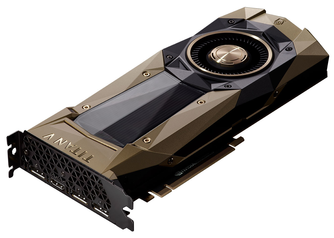
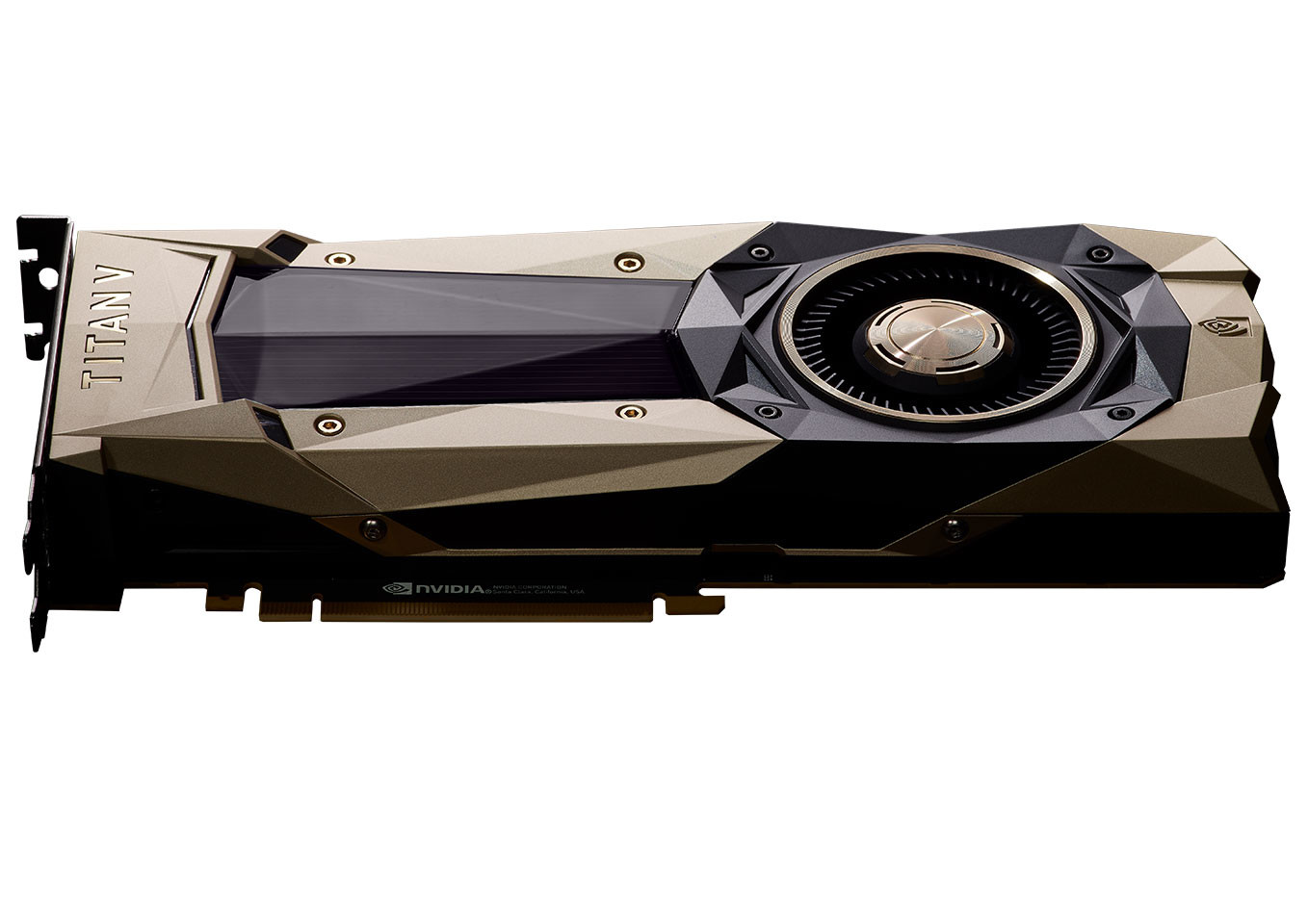
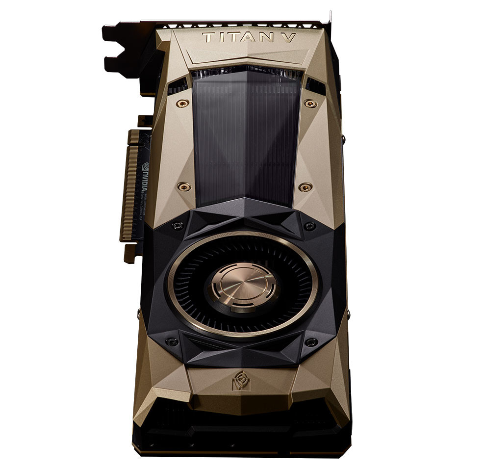
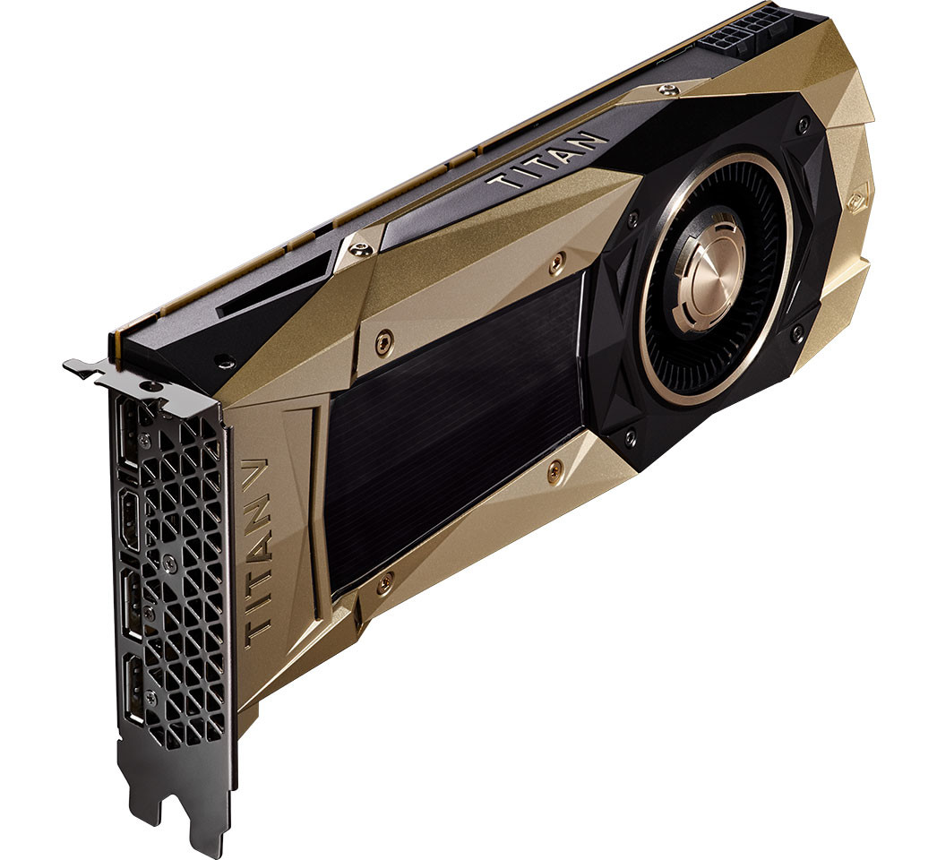
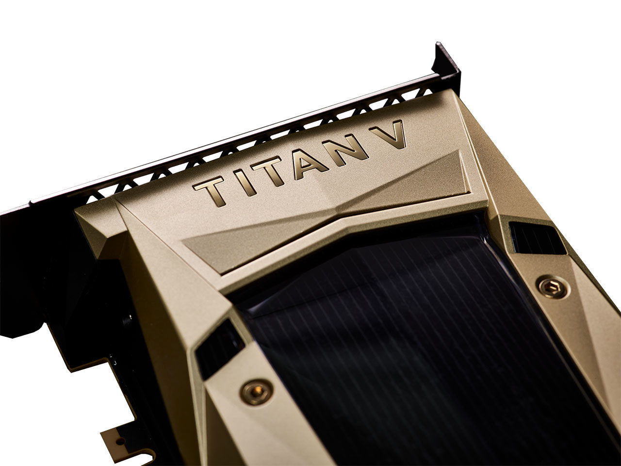
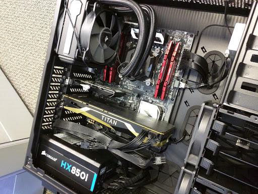
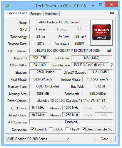
NVIDIA TITAN V Lacks SLI or NVLink Support

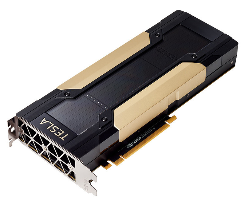
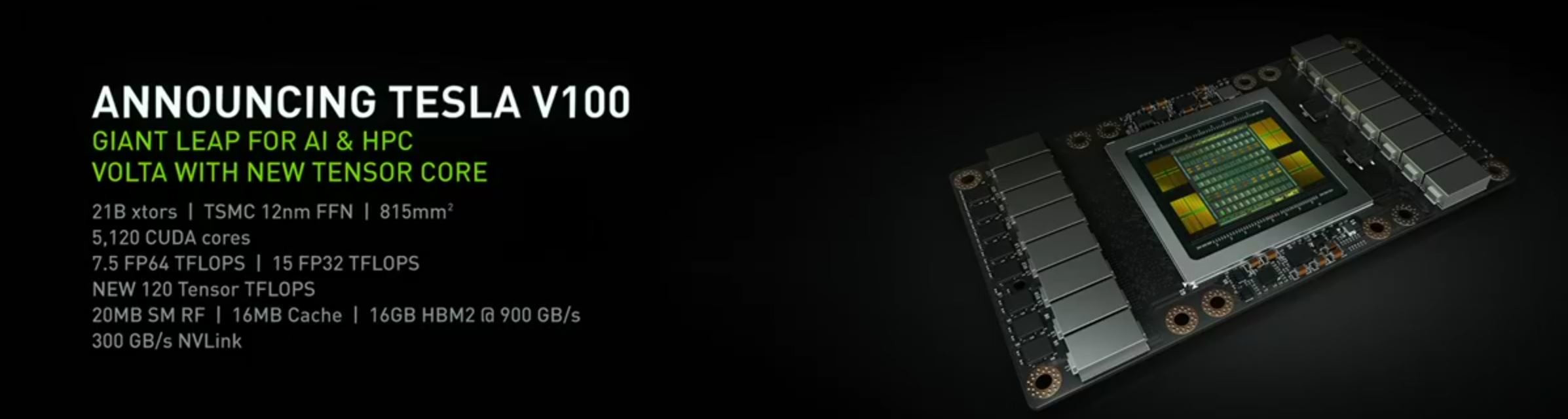
Earlier today, we brought you a story about NVIDIA TITAN V setting you back by up to $7,196 for two cards and two $600 NVLink cables. We got word from NVIDIA that the card neither features NVLink, nor supports SLI, and have since edited it. The NVLink fingers on the TITAN V card are rudiments of the functional NVLink interface found on the Tesla V100 PCIe, being developed by NVIDIA, as the TITAN V, Tesla V100, and a future Quadro GV100 share a common PCB. The NVLink fingers on the TITAN V are concealed by the base-plate of the cooler on one side, and the card's back-plate on the other; so the female connectors of NVLink bridge cables can't be plugged in.

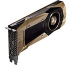
With the lack of SLI support on what is possibly it's fastest graphics card based on the "Volta" architecture, NVIDIA seems to have responded to market trends that multi-GPU is dying or dead. That said, it would be interesting to see if professional overclockers chasing benchmark leaderboard glory pick up the TITAN V, as opposed to two TITAN Xp in SLI or four Radeon RX Vega 64 in 4-way CrossFireX.

NVIDIA Announces TITAN V "Volta" Graphics Card

NVIDIA in a shock move, announced its new flagship graphics card, the TITAN V. This card implements the "Volta" GV100 graphics processor, the same one which drives the company's Tesla V100 HPC accelerator. The GV100 is a multi-chip module, with the GPU die and three HBM2 memory stacks sharing a package. The card features 12 GB of HBM2 memory across a 3072-bit wide memory interface. The GPU die has been built on the 12 nm FinFET+ process by TSMC. NVIDIA TITAN V maxes out the GV100 silicon, if not its memory interface, featuring a whopping 5,120 CUDA cores, 640 Tensor cores (specialized units that accelerate neural-net building/training). The CUDA cores are spread across 80 streaming multiprocessors (64 CUDA cores per SM), spread across 6 graphics processing clusters (GPCs). The TMU count is 320.

The GPU core is clocked at 1200 MHz, with a GPU Boost frequency of 1455 MHz, and an HBM2 memory clock of 850 MHz, translating into 652.8 GB/s memory bandwidth (1.70 Gbps stacks). The card draws power from a combination of 6-pin and 8-pin PCIe power connectors. Display outputs include three DP and one HDMI connectors. With a wallet-scorching price of USD $2,999, and available exclusively through NVIDIA store, the TITAN V is evidence that with Intel deciding to sell client-segment processors for $2,000, it was a matter of time before GPU makers seek out that price-band. At $3k, the GV100's margins are probably more than made up for.

"Summit" Supercomputer to Propel US Back to Number 1 in Top 500 by 2018

China has been increasingly - and steadily - gaining relevance in the supercomputing world, with most of the top-500 entries being controlled by that country. In fact, China can boast of having the number one supercomputer in the world, the Sunway TaihuLight, which can deliver 93 PetaFLOPS of computing power - just 3x more computational power than the second most powerful machine, China's own Tianhe-2). However, supercomputing, and the amount of money that's earned by selling processing slices of these supercomputers for private or state contractors, i a very attractive pull - especially considering the increasingly more expensive computational needs of the modern world.

The Summit is to be the United State's call to fame in that regard, bringing the country back to number one in raw, top-of-the-line single-machine supercomputing power. Summit is promising to more than double the PetaFLOPS of China's TaihuLight, to over 200 PetaFLOPs. That amounts to around 11x more processing grunt than its predecessor, the Titan, in a much smaller footprint - the Titan's 18,688 processing nodes will be condensed to just ~4,600 nodes on the Summit, with each node achieving around 40 TeraFLOPS of computing power. The hardware? IBM and NVIDIA, married in water-cooled nodes with the powerful GV100 accelerator that's still eluding us enthusiasts - but that's a question for another day.

NVIDIA Announces SaturnV AI Supercomputer Powered by "Volta"

NVIDIA at the Supercomputing 2017 conference announced a major upgrade of its new SaturnV AI supercomputer, which when complete, the company claims, will be not just one of the world's top-10 AI supercomputers in terms of raw compute power; but will also the world's most energy-efficient. The SaturnV will be a cluster supercomputer with 660 NVIDIA DGX-1 nodes. Each such node packs eight NVIDIA GV100 GPUs, which takes the machine's total GPU count to a staggering 5,280 (that's GPUs, not CUDA cores). They add up to an FP16 performance that's scraping the ExaFLOP (1,000-petaFLOP or 10^18 FLOP/s) barrier; while its FP64 (double-precision) compute performance nears 40 petaFLOP/s (40,000 TFLOP/s).

SaturnV should beat Summit, a supercomputer being co-developed by NVIDIA and IBM, which in turn should unseat Sunway TaihuLight, that's currently the world's fastest supercomputer. This feat gains prominence as NVIDIA SaturnV and NVIDIA+IBM Summit are both machines built by the American private-sector, which are trying to beat a supercomputing leader backed by the mighty Chinese exchequer. The other claim to fame of SaturnV is its energy-efficiency. Before its upgrade, SaturnV achieved an energy-efficiency of a staggering 15.1 GFLOP/s per Watt, which was already the fourth "greenest." NVIDIA expects the upgraded SaturnV to take the number-one spot.

China Pulls Ahead of U.S. in Latest TOP500 List

The fiftieth TOP500 list of the fastest supercomputers in the world has China overtaking the US in the total number of ranked systems by a margin of 202 to 143. It is the largest number of supercomputers China has ever claimed on the TOP500 ranking, with the US presence shrinking to its lowest level since the list's inception 25 years ago.

Just six months ago, the US led with 169 systems, with China coming in at 160. Despite the reversal of fortunes, the 143 systems claimed by the US gives them a solid second place finish, with Japan in third place with 35, followed by Germany with 20, France with 18, and the UK with 15.

NVIDIA "Volta" Architecture Successor Codenamed "Ampere," Expected GTC 2018

NVIDIA has reportedly codenamed the GPU architecture that succeeds its upcoming "Volta" architecture after the 18th century French physicist who is one of the pioneers of electromagnetism, André-Marie Ampère, after whom the popular unit of measuring current is named. The new NVIDIA "Ampere" GPU architecture, which succeeds "Volta," will make its debut at the 2018 Graphics Technology Conference (GTC), hosted by NVIDIA. As with GPU architecture launches by the company in recent times, one can expect an unveiling of the architecture, followed by preliminary technical presentations by NVIDIA engineers, with actual products launching a little later, and consumer-grade GeForce product launching much later.

NVIDIA is yet to launch GeForce products based on its upcoming "Volta" architecture as its current "Pascal" architecture turns 18 months old in the consumer graphics space. Should NVIDIA continue on the four-digit model number scheme of its GeForce 10-series "Pascal" family, one can expect those based on "Volta" to follow the GeForce 20-series, and "Ampere" GeForce 30-series. NVIDIA is yet to disclose the defining features of the "Ampere" architecture. We'll probably have to wait until March 2018 to find out.

25+ Companies Developing Level 5 Robotaxis on NVIDIA CUDA GPUs

NVIDIA today unveiled the world's first artificial intelligence computer designed to drive fully autonomous robotaxis. The new system, codenamed Pegasus, extends the NVIDIA DRIVE PX AI computing platform to handle Level 5 driverless vehicles. NVIDIA DRIVE PX Pegasus delivers over 320 trillion operations per second -- more than 10x the performance of its predecessor, NVIDIA DRIVE PX 2.

NVIDIA DRIVE PX Pegasus will help make possible a new class of vehicles that can operate without a driver -- fully autonomous vehicles without steering wheels, pedals or mirrors, and interiors that feel like a living room or office. They will arrive on demand to safely whisk passengers to their destinations, bringing mobility to everyone, including the elderly and disabled.

Supermicro Releases Supercharged NVIDIA Volta Systems

Super Micro Computer, Inc. (NASDAQ: SMCI), a global leader in enterprise computing, storage, and networking solutions and green computing technology, today announced support for NVIDIA Tesla V100 PCI-E and V100 SXM2 GPUs on its industry leading portfolio of GPU server platforms.

For maximum acceleration of highly parallel applications like artificial intelligence (AI), deep learning, autonomous vehicle systems, energy and engineering/science, Supermicro's new 4U system with next-generation NVIDIA NVLink is optimized for overall performance. The SuperServer 4028GR-TXRT supports eight NVIDIA Tesla V100 SXM2 GPU accelerators with maximum GPU-to-GPU bandwidth for important HPC clusters and hyper-scale workloads. Incorporating the latest NVIDIA NVLink GPU interconnect technology with over five times the bandwidth of PCI-E 3.0, this system features an independent GPU and CPU thermal zoning design, which ensures uncompromised performance and stability under the most demanding workloads.

NVIDIA Announces OptiX 5.0 SDK - AI-Enhanced Ray Tracing

At SIGGRAPH 2017, NVIDIA introduced the latest version of their AI-based, GPU-enabled ray-tracing OptiX API. The company has been at the forefront of GPU-powered AI endeavors in a number of areas, including facial animation, anti-aliasing, denoising, and light transport. OptiX 5.0 brings a renewed focus on AI-based denoising.

AI training is still a brute-force scenario with finesse applied at the end: basically, NVIDIA took tens of thousands of image pairs of rendered images with one sample per pixel and a companion image of the same render with 4,000 rays per pixel, and used that to train the AI to predict what a denoised image looks like. Basically (and picking up the numbers NVIDIA used for its AI training), this means that in theory, users deploying OptiX 5.0 only need to render one sample per pixel of a given image, instead of the 4,000 rays per pixel that would be needed for its final presentation. Based on its learning, the AI will then be able to fill in the blanks towards finalizing the image, saving the need to render all that extra data. NVIDIA quotes a 157x improvement in render time using a DGX station with Optix 5.0 deployed against the same render on a CPU-based platform (2 x E5-2699 v4 @ 2.20GHz). The Optix 5.0 release also includes provisions for GPU-accelerated motion blur, which should do away with the need to render a frame multiple times and then applying a blur filter through a collage of the different frames. NVIDIA said OptiX 5.0 will be available in November. Check the press release after the break.

NVIDIA CEO Gives Away First Tesla V100 Accelerators to Top AI Researchers

NVIDIA CEO over the weekend, held a special event recognizing the efforts of some of the world's foremost AI researchers, and gifted each one of them the first production Tesla V100 GPU compute accelerators. Based on the company's latest "Volta" GPU architecture, the V100 features special "tensor cores," components that speed up deep-learning neural net training, which should have a significant impact on AI research as it cuts down hours or even days of neural net training in a typical project.

At the NVAIL (NVIDIA AI Labs) meetup hosted by NVIDIA, CEO Jen Hsun Huang stressed on the importance of supporting AI research. "AI is the most powerful technology force that we have ever known," said Jen Hsun, "I've seen everything. I've seen the coming and going of the client-server revolution. I've seen the coming and going of the PC revolution. Absolutely nothing compares," he said.

NVIDIA Announces the Tesla V100 PCI-Express HPC Accelerator

NVIDIA formally announced the PCI-Express add-on card version of its flagship Tesla V100 HPC accelerator, based on its next-generation "Volta" GPU architecture. Based on the advanced 12 nm "GV100" silicon, the GPU is a multi-chip module with a silicon substrate and four HBM2 memory stacks. It features a total of 5,120 CUDA cores, 640 Tensor cores (specialized CUDA cores which accelerate neural-net building), GPU clock speeds of around 1370 MHz, and a 4096-bit wide HBM2 memory interface, with 900 GB/s memory bandwidth. The 815 mm² GPU has a gargantuan transistor-count of 21 billion. NVIDIA is taking institutional orders for the V100 PCIe, and the card will be available a little later this year. HPE will develop three HPC rigs with the cards pre-installed.

NVIDIA's Market Cap to Reach $100 billion Soon; Grew ~$25 billion Since May 2017

NVIDIA has been on a roll lately with their market capitalization and share valuation, which could very well send the company soaring past the $100 billion dollar mark today. Whether or not that happens (and if it does, it will be a historical milestone for the company), NVIDIA's growth of almost $25 billion dollars since May 13th is nothing short of jaw-dropping.

The "sudden" market valuation on NVIDIA comes on the heels of the company's strong graphics execution and increasingly entrenched position in the high performance GPU computing market for machine learning. The company's Volta architecture, which was showcased by Jensen Huang at their GTC keynote on May 10th, boosted confidence in the company significantly. Since then, the company's market cap has increased from the $75 billion dollar it was at shortly after GTC, towards its $96.31 billion rated market cap today. More recently, with the recent rise of the crypto wave craze, NVIDIA's GPUs have been talked about as real alternatives to AMD's previously (and perhaps hurtful for the company) grasp on this kind of workloads.

Could This be the NVIDIA TITAN Volta?

NVIDIA, which unveiled its faster "Volta" GPU architecture at its 2017 Graphics Technology Conference (GTC), beginning with the HPC product Tesla V100, is closer to launching the consumer graphics variant, the TITAN Volta. A curious-looking graphics card image with "TITAN" markings surfaced on Reddit. One could discount the pic for being that of a well-made cooler mod, until you take a peak at the PCB. It appears to lack SLI fingers where you'd expect them to be, and instead has NVLink fingers in positions found on the PCIe add-in card variant of the Tesla P100 HPC accelerator.

You might think "alright, it's not a fancy TITAN X Pascal cooler mod, but it could be a P100 with a cooler mod," until you notice the power connectors - it has two power inputs on top of the card (where they're typically found on NVIDIA's consumer graphics cards), and not the rear portion of the card (where the P100 has it, and where they're typically found on Tesla and Quadro series products). Whoever pulled this off has done an excellent job either way - of scoring a potential TITAN Volta sample, or modding whatever card to look very plausible of being a TITAN Volta.

NVIDIA Announces Its Volta-based Tesla V100

Today at its GTC keynote, NVIDIA CEO Jensen Huang took the wraps on some of the features on their upcoming V100 accelerator, the Volta-based accelerator for the professional market that will likely pave the way to the company's next-generation 2000 series GeForce graphics cards. If NVIDIA goes on with its product carvings and naming scheme for the next-generation Volta architecture, we can expect to see this processor on the company's next-generation GTX 2080 Ti. Running the nitty-gritty details (like the new Tensor processing approach) on this piece would be impossible, but there are some things we know already from this presentation.

This chip is a beast of a processor: it packs 21 billion transistors (up from 15,3 billion found on the P100); it's built on TSMC's 12 nm FF process (evolving from Pascal's 16 nm FF); and measures a staggering 815 mm² (from the P100's 610 mm².) This is such a considerable leap in die-area that we can only speculate on how yields will be for this monstrous chip, especially considering the novelty of the 12 nm process that it's going to leverage. But now, the most interesting details from a gaming perspective are the 5,120 CUDA cores powering the V100 out of a total possible 5,376 in the whole chip design, which NVIDIA will likely leave for their Titan Xv. These are divided in 84 Volta Streaming Multiprocessor Units with each carrying 64 CUDA cores (84 x 64 = 5,376, from which NVIDIA is cutting 4 Volta Streaming Multiprocessor Units for yields, most likely, which accounts for the announced 5,120.) Even in this cut-down configuration, we're looking at a staggering 42% higher pure CUDA core-count than the P100's. The new V100 will offer up to 15 FP 32 TFLOPS, and will still leverage a 16 GB HBM2 implementation delivering up to 900 GB/s bandwidth (up from the P100's 721 GB/s). No details on clock speed or TDP as of yet, but we already have enough details to enable a lengthy discussion... Wouldn't you agree?

NVIDIA's Volta Reportedly Poised for Anticipated, Early Q3 2017 Launch

According to a report from Chinese website MyDrivers, NVIDIA is looking to spruce things up on its line-up with a much earlier than expected Q3 Volta Launch. Remember that Volta was expected, according to NVIDIA's own road-maps, to launch around early 2018. The report indicates that NVIDIA's Volta products - apparently to be marketed as the GeForce 20-series - will see an early launch due to market demands, and NVIDIA's intention to further increase pricing of its products through a new-generation launch.

These stand, for now, as only rumors (and not the first time they've surfaced at that), but paint a pretty interesting picture, nonetheless. Like Intel with its Coffee Lake series, pushing a product launch to earlier than expected has consequences: production, logistics, infrastructure, product roadmaps, and stock of existing previous-generation products must all be taken into account. And with NVIDIA just recently having introduced its performance-champions GTX 1080 Ti and Titan Xp graphics cards, all of this seems a trigger pull too early - especially when taking into account the competition landscape in high-performance graphics, which is akin to a single green-colored banner poised atop the Himalayas. And NVIDIA must not forget the fact that AMD could be pulling a black swan off its engineering department with Vega, like it did with its Ryzen series of CPUs.

NVIDIA to Build "Volta" Consumer GPUs on TSMC 12 nm Process

NVIDIA's next-generation "Volta" GPU architecture got its commercial debut in the most unlikely class of products, with the Xavier autonomous car processor. The actual money-spinners based on the architecture, consumer GPUs, will arrive some time in 2018. The company will be banking on its old faithful fab TSMC, to build those chips on a new 12 nanometer FinFET node that's currently under development. TSMC's current frontline process is the 16 nm FFC, which debuted in mid-2015, with mass-production following through in 2016. NVIDIA's "GP104" chip is built on this process.

This could also mean that NVIDIA could slug it out against AMD with its current GeForce GTX 10-series "Pascal" GPUs throughout 2017-18, even as AMD threatens to disrupt NVIDIA's sub-$500 lineup with its Radeon Vega series, scheduled for Q2-2017. NVIDIA's "Volta" architecture could see stacked DRAM technologies such as HBM2 gain more mainstream exposure, although competing memory standards such as GDDR6 aren't too far behind.

On NVIDIA's Tile-Based Rendering

Looking back on NVIDIA's GDC presentation, perhaps one of the most interesting aspects approached was the implementation of tile-based rendering on NVIDIA's post-Maxwell architectures. This has been an adaptation of typically mobile approaches to graphics rendering which keeps their specific needs for power efficiency in mind - and if you'll "member", "Maxwell" was NVIDIA's first graphics architecture publicly touted for its "mobile first" design.

This approach essentially divides the screen into tiles, and then rasterizes the entire frame in a per-tile basis. 16×16 and 32×32 pixels are the usual tile sizes, but both Maxwell and Pascal can dynamically assess the required tile size for each frame, changing it on-the-fly as needed and according to the complexity of the scene. This looks to ensure that the processed data has a much smaller footprint than that of the full image rendering - small enough that it makes it possible for NVIDIA to keep the data in a much smaller amount of memory (essentially, the L2 memory), dynamically filling and flushing the available cache as possible until the full frame has been rendered. This means that the GPU doesn't have to access larger, slower memory pools as much, which primarily reduces the load on the VRAM subsystem (increasing available VRAM for other tasks), whilst simultaneously accelerating rendering speed. At the same time, a tile-based approach also lends itself pretty well to the nature of GPUs - these are easily parallelized operations, with the GPU being able to tackle many independent tiles simultaneously, depending on the available resources.

NVIDIA Announces Xavier, Volta-based Autonomous Transportation SoC

At its inaugural European edition of the Graphics Technology Conference (GTC), NVIDIA announced Xavier, an "AI supercomputer for the future of autonomous transportation." An evolution of its Drive PX2 board that leverages a pair of "Maxwell" GPUs with some custom logic and an ARM CPU, to provide cars with the compute power necessary to deep-learn the surroundings and self-drive, or assist-drive; Xavier is a refinement over Drive PX2 in that it merges three chips - two GPUs and one control logic into an SoC.

You'd think that NVIDIA refined its deep-learning tech enough to not need a pair of "Maxwell" SoCs, but Xavier is more than that. The 7 billion-transistor chip built on 16 nm FinFET process, offers more raw compute performance thanks to leveraging NVIDIA's next-generation "Volta" architecture, one more advanced than even its current "Pascal" architecture. The chip features a "Volta" GPU with 512 CUDA cores. The CVA makes up the vehicle I/O, while an image processor that's capable of 8K HDR video streams feeds the chip with visual inputs from various cameras around the vehicle. An 8-core ARM CPU performs general-purpose compute. NVIDIA hopes to get the first engineering samples of Xavier out to interested car-makers by Q4-2017.

NVIDIA Accelerates Volta to May 2017?

Following the surprise TITAN X Pascal launch slated for 2nd August, it looks like NVIDIA product development cycle is running on steroids, with reports emerging of the company accelerating its next-generation "Volta" architecture debut to May 2017, along the sidelines of next year's GTC. The architecture was originally scheduled to make its debut in 2018.

Much like "Pascal," the "Volta" architecture could first debut with HPC products, before moving on to the consumer graphics segment. NVIDIA could also retain the 16 nm FinFET+ process at TSMC for Volta. Stacked on-package memory such as HBM2 could be more readily available by 2017, and could hit sizable volumes towards the end of the year, making it ripe for implementation in high-volume consumer products.

NVIDIA Coming Around to Vulkan Support

NVIDIA is preparing to add support for Vulkan, the upcoming 3D graphics API by Khronos, and successor to OpenGL, to its feature-set. The company's upcoming GeForce 358.66 series driver will introduce support for Vulkan. What makes matters particularly interesting is the API itself. Vulkan is heavily based on AMD's Mantle API, which the company gracefully retired in favor of DirectX 12, and committed its code to Khronos. The 358 series drivers also reportedly feature function declarations in their CUDA code for upcoming NVIDIA GPU architectures, such as Pascal and Volta.

Cyberpower Makes New V3 Voltair CPU Cooler Available in Custom-Built PCs

Cyberpower Inc., a global manufacturer of custom gaming PCs, gaming laptops, and performance workstations, has entered into an agreement with V3 Components to be the exclusive distributor of V3 Components products in North America. V3 Components, based in Lomita, California is a new manufacturer of enthusiast level computer components. The company recently announced its first product, the V3 Voltair High Performance Thermoelectric CPU Cooler.

"We are very happy to have Cyberpower Inc. as the exclusive distributor of our products in North America. Cyberpower Inc. offers the logistics capacity and market reach to help make our products available to a much wider audience than we would be able to on our own," said Chuck Morris, Product Manager at V3 Components. "Cyberpower Inc. has successful partnerships among both etailers and the retail channel that it will use to offer V3 Components products to customers.

TechPowerUp GPU-Z 0.7.6 Released

TechPowerUp released GPU-Z version 0.7.6, the latest version of the popular lightweight graphics subsystem information, monitoring, and diagnostic utility. Version 0.7.6 comes with support for new GPUs, including NVIDIA's upcoming Maxwell architecture. It also introduces the ability to tell the vendor of memory chips on your discrete graphics card, and a reliable new BIOS reading method for NVIDIA GPUs.

To begin with, GPU-Z adds support for NVIDIA's upcoming GeForce GTX TITAN Black, GeForce GTX 750 Ti, GTX 750 (non-Ti), both of which are based on NVIDIA's "Maxwell" micro-architecture, GTX 840M, and new GTX 760 "lite" (192-bit). On the AMD front, it adds support for AMD A-Series "Kaveri" iGPUs, Radeon R7 M265, FireStream 9350, HD 8530M, and HD 8650D. A new Intel Iris Pro 5200 variant is supported.

GPU-Z 0.7.6 comes with a revolutionary new feature, the ability to tell the vendor of the memory chips on your graphics card, so you don't have to take your card apart to tell the same. GPU-Z 0.7.6 also integrates NVIDIA NVFlash to reliably read BIOS of NVIDIA GPUs. Voltage monitoring of GeForce GTX 780 Ti is improved.
DOWNLOAD: TechPowerUp GPU-Z 0.7.6 | TechPowerUp GPU-Z 0.7.6 ASUS ROG Edition

The change-log follows.

G.Skill Announces Ripjaws SO-DIMM Series

G.SKILL International Co. Ltd., the leading high performance memory designer and manufacturer, adds a brand new DDR3 SO-DIMM Series to its product line, named G.SKILL Ripjaws DDR3 SO-DIMM Memory. Besides using only highly selected components, every G.SKILL Ripjaws SO-DIMM memory kit is 100% validated with G.SKILL rigorous burn-in tests. It ensures every Ripjaws SO-DIMM kit delivers perfect stability, performance, and quality for your notebook and PC.

NVIDIA Updates GPU Roadmap with "Volta"

NVIDIA updated its GPU micro-architecture roadmap at the 2013 GPU Technology Conference (GTC). Currently spearheaded by the "Kepler" micro-architecture, which drives its GeForce, Quadro, and Tesla product lines, and which will drive Tegra mobile SoCs in 2014; NVIDIA's next-generation "Maxwell" could make its debut some time in 2014. Going by NVIDIA's graph that puts performance-per-Watt against time, "Maxwell" should nearly double performance. Maxwell GPUs feature unified virtual memory, which lets CPUs treat graphics card memory as system memory, for faster general-purpose performance.

Although not backed by a tentative launch year, and assuming "Maxwell" has its run for another two years, 2016 could see the launch of NVIDIA's "Volta" GPU micro-architecture. In addition to advancements by its predecessors, "Volta" could introduce stacked DRAM technology. It would enable GPU memory bandwidths as high as 1 TB/s. Current high-end graphics cards such as GeForce Titan and Radeon HD 7970 GHz Edition, are capable of breaching the 300 GB/s mark, so NVIDIA's claims don't sound far-fetched.
Return to Keyword Browsing
Apr 23rd, 2024 07:58 EDT change timezone

New Forum Posts

Popular Reviews

Controversial News Posts