 301
301
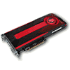
AMD Radeon HD 7970 3 GB Review
Architecture »Introduction
Out with the old, in with the new. Let's welcome the newest kid on the block, the Radeon HD 7970, part of AMD's spanking new Southern Islands GPU family. This card is the industry's first with a few things, it uses the first ever high-performance GPU built on the 28 nanometer silicon fabrication process; Radeon HD 7970 is the industry's first card compliant with Microsoft's DirectX 11.1 API, which will ship with the next major version of Windows; and is the first card to use the PCI Express 3.0 x16 bus, that doubles system interface bandwidth to 32 Gb/s and is touted by motherboard manufacturers as the next big thing since PCI.
New generations of GPUs naturally bring with them performance increments, some times even 100% that of preceding generations, they also serve as launch-vehicles for new features that quickly go on to become industry standards, and help the technology grow. The Radeon HD 7970 has both of these responsibilities resting on its shoulders: to score performance wins, and pack some killer new features that matter to the end-user.

Product Positioning
The AMD Radeon HD 7970 is a unique card from a market-positioning standpoint. After Radeon HD 2900 series, and the completion of ATI's merger with AMD, the company took up a unique model of product development that ensured it could have competitive products out in the market targeting every segment, while not having to spend much on making large GPUs. Its goal with a new GPU architecture always involved making a killer high-performance (not high-end) GPU, and using it both ways: in dual-GPU cards as high-end products, and by disabling some components/features to carve out cheaper/cost-effective products.The AMD Radeon HD 7970, particularly the GPU behind it, codenamed "Tahiti", is stretching that model a little towards the higher-end. Tahiti is bigger than what AMD's typical "high-performance" GPU is supposed to be. For one, it features a 384-bit wide memory interface. AMD was the first to market with GDDR5 memory standard, which it initially sought as a way to circumvent the need for a GDDR3/4 memory bus wider than 256-bits. With NVIDIA catching up with the memory standard, and implementing a 384-bit GDDR5 memory interface on its GeForce Fermi 100/110 GPUs, AMD felt the pinch for doing something to increase the memory bandwidth of the HD 7970, to keep up with the increasing compute performance of their GPUs. The company chose slightly faster GDDR5 memory chips with HD 6900 series, but it could only yield small bandwidth gains. The only option left without having to switch memory architecture to the lesser known XDR2, was to increase the memory bus width physically by 50%, hence 384-bit. Coupled with the faster 5.5 GT/s memory chips it used on the HD 6900, and appropriate clock speeds, it yields around 260 GB/s of memory bandwidth.

The unconventionally-wider memory bus of the Radeon HD 7970, combined with a brand new math-processing machinery contribute to the HD 7970's product placement, which is between the previous-generation single-GPU Radeon HD 6970, and previous-generation dual-GPU HD 6990, tilting closer towards the HD 6990.
| GeForce GTX 560 | GeForce GTX 560 Ti | GeForce GTX 560 Ti 448 C | Radeon HD 6950 | GeForce GTX 570 | Radeon HD 6970 | GeForce GTX 580 | Radeon HD 7970 | Radeon HD 6990 | GeForce GTX 590 | ||
|---|---|---|---|---|---|---|---|---|---|---|---|
| Shader Units | 336 | 384 | 448 | 1408 | 480 | 1536 | 512 | 2048 | 2x 1536 | 2x 512 | |
| ROPs | 32 | 32 | 40 | 32 | 40 | 32 | 48 | 32 | 2x 32 | 2x 48 | |
| Graphics Processor | GF114 | GF114 | GF110 | Cayman | GF110 | Cayman | GF110 | Tahiti | 2x Cayman | 2x GF110 | |
| Transistors | 1950M | 1950M | 3000M | 2640M | 3000M | 2640M | 3000M | 4310M | 2x 2640M | 2x 3000M | |
| Memory Size | 1024 MB | 1024 MB | 1280 MB | 2048 MB | 1280 MB | 2048 MB | 1536 MB | 3072 MB | 2x 2048 MB | 2x 1536 MB | |
| Memory Bus Width | 256 bit | 256 bit | 320 bit | 256 bit | 320 bit | 256 bit | 384 bit | 384 bit | 2x 256 bit | 2x 384 bit | |
| Core Clock | 810 MHz | 823 MHz | 732 MHz | 800 MHz | 732 MHz | 880 MHz | 772 MHz | 925 MHz | 830 MHz | 607 MHz | |
| Memory Clock | 1002 MHz | 1002 MHz | 950 MHz | 1250 MHz | 950 MHz | 1375 MHz | 1002 MHz | 1375 MHz | 1250 MHz | 855 MHz | |
| Price | $180 | $210 | $290 | $250 | $330 | $340 | $500 | $549 | $700 | $750 |
Apr 25th, 2024 12:37 EDT
change timezone
Latest GPU Drivers
New Forum Posts
- Meta Horizon OS (20)
- WCG Daily Numbers (12497)
- Share your AIDA 64 cache and memory benchmark here (2917)
- Best SSD for system drive (76)
- Ghetto Mods (4319)
- How to check flatness of CPUs and coolers - INK and OPTICAL INTERFERENCE methods (110)
- Have you got pie today? (16317)
- Milestones (13874)
- TPU's Rosetta Milestones and Daily Pie Thread (1859)
- ThrottleStop 9.6 Voltage won't change (4)
Popular Reviews
- Fractal Design Terra Review
- Thermalright Phantom Spirit 120 EVO Review
- Corsair 2000D Airflow Review
- Minisforum EliteMini UM780 XTX (AMD Ryzen 7 7840HS) Review
- ASUS GeForce RTX 4090 STRIX OC Review
- NVIDIA GeForce RTX 4090 Founders Edition Review - Impressive Performance
- ASUS GeForce RTX 4090 Matrix Platinum Review - The RTX 4090 Ti
- MSI GeForce RTX 4090 Suprim X Review
- MSI GeForce RTX 4090 Gaming X Trio Review
- Gigabyte GeForce RTX 4090 Gaming OC Review
Controversial News Posts
- Sony PlayStation 5 Pro Specifications Confirmed, Console Arrives Before Holidays (116)
- NVIDIA Points Intel Raptor Lake CPU Users to Get Help from Intel Amid System Instability Issues (106)
- AMD "Strix Halo" Zen 5 Mobile Processor Pictured: Chiplet-based, Uses 256-bit LPDDR5X (101)
- US Government Wants Nuclear Plants to Offload AI Data Center Expansion (98)
- Windows 11 Now Officially Adware as Microsoft Embeds Ads in the Start Menu (94)
- AMD's RDNA 4 GPUs Could Stick with 18 Gbps GDDR6 Memory (85)
- Developers of Outpost Infinity Siege Recommend Underclocking i9-13900K and i9-14900K for Stability on Machines with RTX 4090 (85)
- Windows 10 Security Updates to Cost $61 After 2025, $427 by 2028 (84)