 29
29
AMD Vega Microarchitecture Technical Overview
Complete Presentation Deck »Performance and Power Management
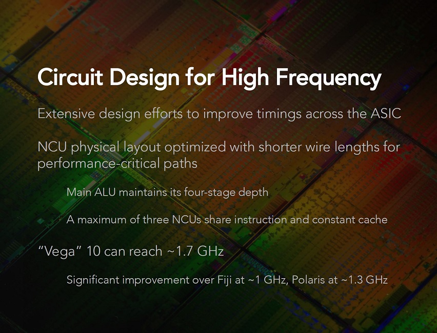
Having spoken to RTG members over the course of the weekend, it seems obvious that a good fraction of the 12.5 billion transistor count was dedicated to increasing the base and boost clocks Vega is capable of relative to Polaris, and also Fiji, which is a direct comparison given their die sizes. As such, AMD is targeting GPU core frequencies on the order of 1.7 GHz with Vega 10, which is a huge improvement over the previous two microarchitectures and can help tremendously if IPC is on par with the highly overclockable NVIDIA GP104 die-based cards. This increased transistor count coupled with a smaller die size relative to Fiji is a result of an optimized general-purpose register design with Vega, wherein AMD claims collaboration with their Ryzen CPU team to have helped with the transistor density and power savings. For example, the company leveraged Globalfoundries' planar transistor technologies, which enables the use of wider transistors when the designer chooses to do so without compromising leakage or parasitics. AMD has also used improved synthesis tools for their circuit design and paid closer attention to their cell library.

AMD also updated the GPU hierarchy such that it improves performance of programs that use deferred shading. The geometry pipeline, the compute engine, and the pixel engine, which output to the ROPs (L1 cache), are now tied to the L2 cache, which has in turn been doubled from 2 MB to 4 MB to cater to these changes.


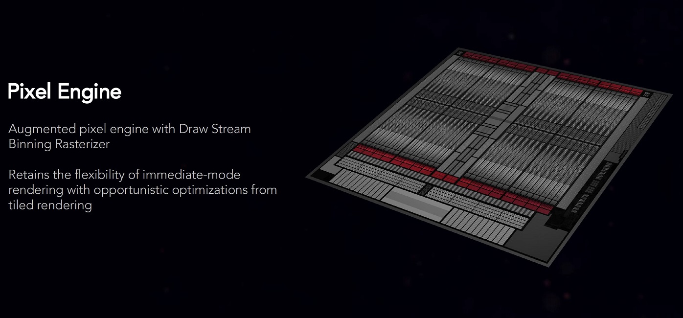
Ahh, it was only a few weeks ago when AMD announced the launch of the Radeon Vega Frontier Edition, and tests quickly revealed that draw-stream binning rasterization (DBSR) was not enabled on it despite the Vega architecture supporting it. AMD today confirmed that Vega 10 does indeed support it and that RX Vega SKUs should too. We are not sure yet if there will be a Radeon Pro software driver update to help enable it with the prosumer Vega Frontier Edition at this point.
DBSR is a tile-based pixel-shading/rendering approach wherein the GPU can render more complex pixels very efficiently relative to previous generations. This is done by having the GPU fetch overlaps only once, followed by performing the pixel-shade of those overlaps only once. As such, any overlapped or invisible pixels are not shaded/rendered, thus saving power and time. AMD has provided some internal testing results to help demonstrate said power savings and performance benefits in synthetic and real-world rendering loads.


The power savings with Vega continue with the addition of an updated micro-controller unit (SMC MCU) for power management alone. Vega supports Infinity Fabric, although in ways yet unknown completely, but one of the ways the MCU aids is by improving idle state power draw - switching over to a sleep state for the GPU core as well as an ultra low operating frequency for the HBM2 memory. AMD is using a very old 3DMark application, Perlin Noise, to generate solid procedural textures in order to demonstrate the power savings in action. This does seem like a stretch, but quantifying idle behavior is not easy to begin with.
Apr 19th, 2024 20:00 EDT
change timezone
Latest GPU Drivers
New Forum Posts
- AMD RX 7000 series GPU Owners' Club (1068)
- I just succesfully baked DDR4 (69)
- I9 13890HX undervolting Suggestions (4)
- Undervolting Dell XPS 14 9440 is it possible? (7)
- Share your AIDA 64 cache and memory benchmark here (2884)
- Roccat Kone AIMO has developed a double left click, when I click it once. Any fix out there? (34)
- The TPU UK Clubhouse (24738)
- XFX RX580 stock Bios (7)
- Looks like the Z80 is finished (2)
- AAF Optimus DCH Audio Modded Driver for Windows 10/11 - For ALL HDAUDIO Enumerator Chips (642)
Popular Reviews
- Horizon Forbidden West Performance Benchmark Review - 30 GPUs Tested
- PowerColor Radeon RX 7900 GRE Hellhound Review
- Fractal Design Terra Review
- Corsair 2000D Airflow Review
- Thermalright Phantom Spirit 120 EVO Review
- Minisforum EliteMini UM780 XTX (AMD Ryzen 7 7840HS) Review
- Creative Pebble X Plus Review
- FiiO KB3 HiFi Mechanical Keyboard Review - Integrated DAC/Amp!
- ASUS GeForce RTX 4090 STRIX OC Review
- NVIDIA GeForce RTX 4090 Founders Edition Review - Impressive Performance
Controversial News Posts
- Sony PlayStation 5 Pro Specifications Confirmed, Console Arrives Before Holidays (111)
- NVIDIA Points Intel Raptor Lake CPU Users to Get Help from Intel Amid System Instability Issues (102)
- US Government Wants Nuclear Plants to Offload AI Data Center Expansion (98)
- AMD "Strix Halo" Zen 5 Mobile Processor Pictured: Chiplet-based, Uses 256-bit LPDDR5X (83)
- Windows 10 Security Updates to Cost $61 After 2025, $427 by 2028 (82)
- Developers of Outpost Infinity Siege Recommend Underclocking i9-13900K and i9-14900K for Stability on Machines with RTX 4090 (82)
- TechPowerUp Hiring: Reviewers Wanted for Motherboards, Laptops, Gaming Handhelds and Prebuilt Desktops (72)
- Intel Realizes the Only Way to Save x86 is to Democratize it, Reopens x86 IP Licensing (70)