 47
47
ASUS ARES 4 GB Review
Test Setup »A Closer Look


The first part that comes off is the cooling plate on the back of the card. It cools only the memory chips on that side and adds additional protection to components of the card. Another aspect is that heat migrates from the GPUs to through the PCB, so cooling on this side helps a bit too.


Next we removed the fan shroud. Unlike all the other fan shrouds I have seen so far, this one is made from metal and covered with a robust powdercoating paint job.


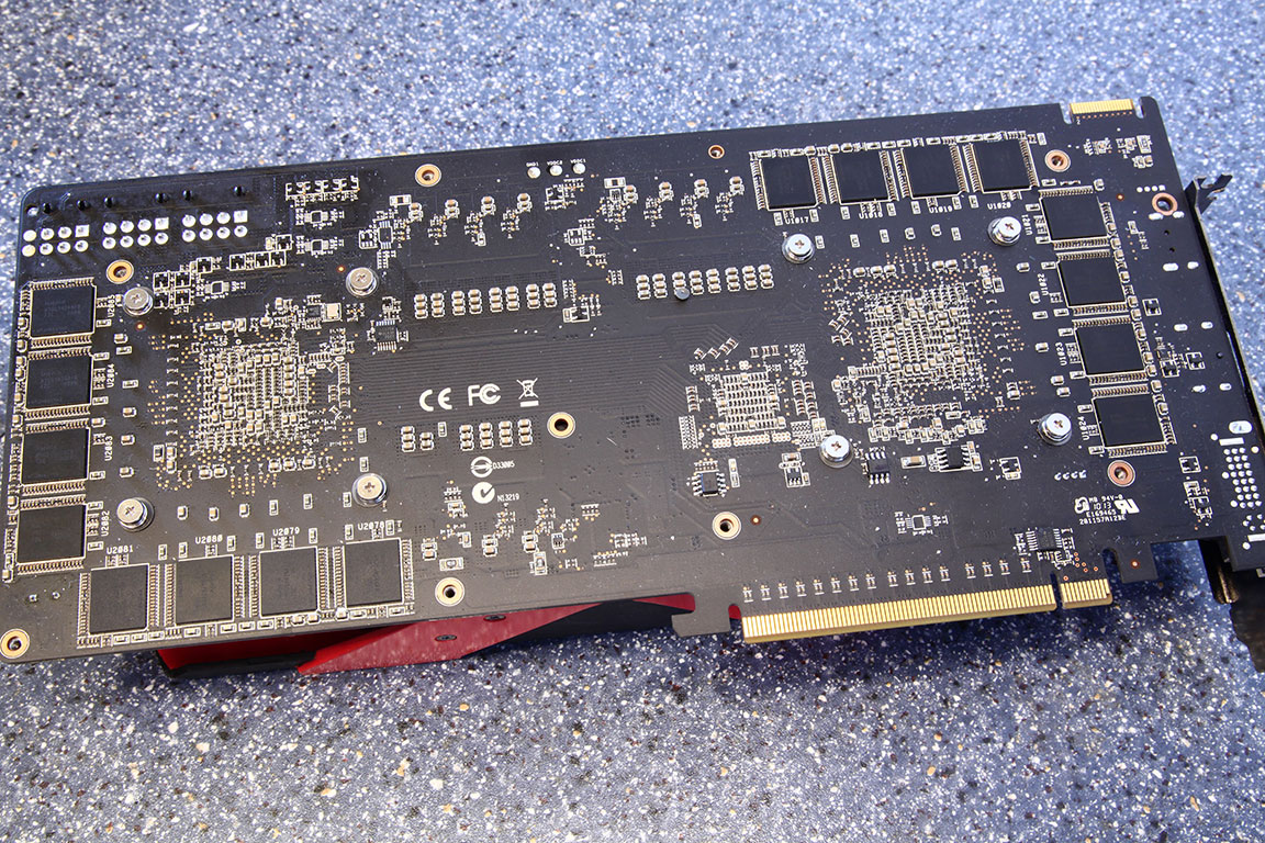
Now you can take a closer look at how the ARES thermal solution works. A central fan creates airflow through the fins of two copper heatsinks that sit on each GPU.
Each of these blocks is made from 100% copper and uses four heatpipes to move heat away from the GPU cores to the fins in its upper portion, where heat is dissipated in the fan's airflow.


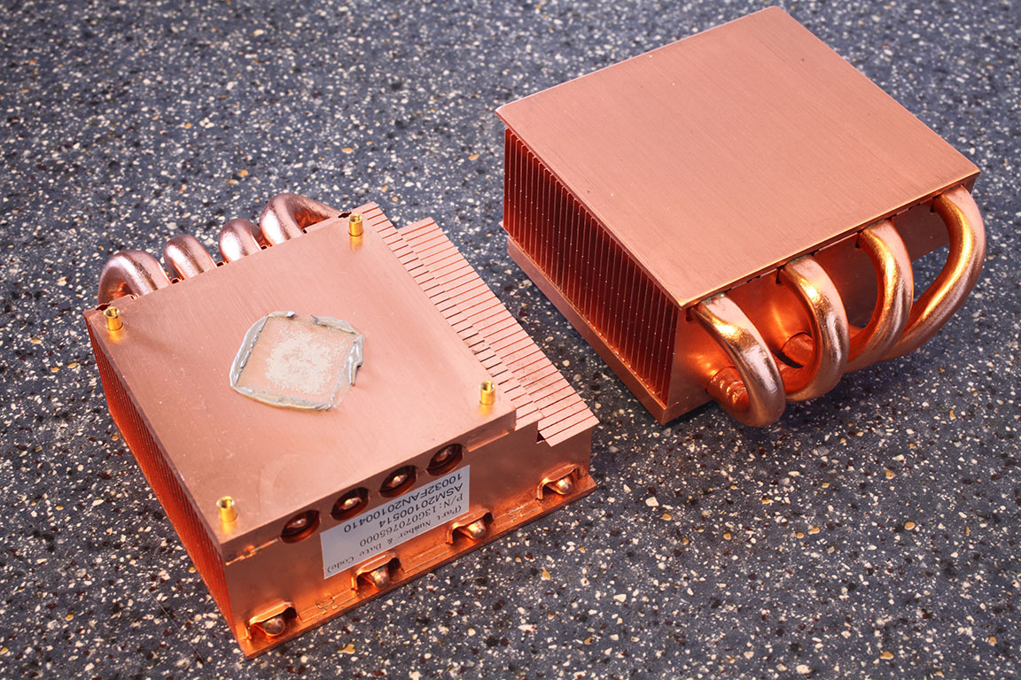
The last piece to come off is this black cooling plate that covers all secondary heat sources like memory chips and voltage regulation circuitry. This multiple component approach is extremely useful to extreme overclockers who use watercooling or LN2. They can focus on cooling the GPUs and use pieces of the stock heatsink to cool the other components, which is usually good enough.
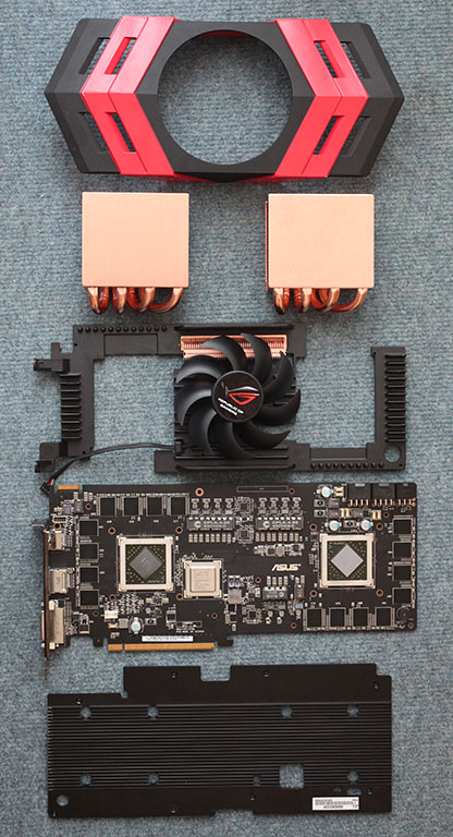
Here you can see all the components that make up the ASUS ARES.

Wow! ASUS has equipped their card with two 8-pin and one 6-pin power connector, and you need them all to run the card. This configuration provides at least 450W power (150W (8 pin) + 150W (8 pin) + 75W (6 pin) + 75 W (slot)).
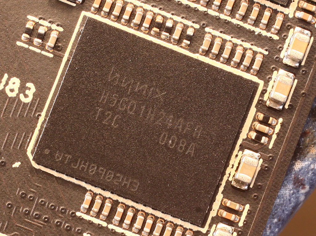
The GDDR5 memory chips are made by Hynix, and carry the model number H5GQ1H24AFR-T2C. They are specified to run at 1250 MHz (5000 MHz GDDR5 effective).

The voltage regulation circuitry is quite extensive and seems to be an upscaled version of the HD 5970 reference design. You have two Volterra VT1165 voltage regulators for the GPU voltage and a third VT1165 for VDDCI. Whereas the HD 5970 uses a 3+1+1 phase configuration per GPU, the ARES uses 4+1+1.

The PCI-Express bridge chip which connects the two GPUs and interfaces with the system via PCI-Express 2.0 is made by PLX. Apparently PLX lets ATI rebrand their product. According to AMD the bridge chip supports PCI-Express 2.1 x16 which supplies enough bandwidth to both GPUs for any situation.


AMD's Cypress GPU comes with 2154 million transistors and is produced on a 40 nm process at TSMC Taiwan. The ARES uses two of these beasts running in an internal CrossFire configuration.
Apr 25th, 2024 16:25 EDT
change timezone
Latest GPU Drivers
New Forum Posts
- Ghetto Mods (4322)
- Legion Pro 7i, i9-13900HX. PL2 limit reason in log file (0)
- What software are you using to monitor CPU temps during gaming session? (14)
- im new to throttelstop and i think i messed it up by copying others any hints would be very much aprreciated (2)
- Alphacool CORE 1 CPU block - bulging with danger of splitting? (15)
- What are you playing? (20528)
- What phone you use as your daily driver? And, a discussion of them. (1480)
- Black screen after muting (4)
- Micron f-die overclock issues (0)
- Will a RTX 4070 TI super bottleneck a Ryzen 9 7950X3D? (59)
Popular Reviews
- Fractal Design Terra Review
- Thermalright Phantom Spirit 120 EVO Review
- Corsair 2000D Airflow Review
- Minisforum EliteMini UM780 XTX (AMD Ryzen 7 7840HS) Review
- ASUS GeForce RTX 4090 STRIX OC Review
- NVIDIA GeForce RTX 4090 Founders Edition Review - Impressive Performance
- ASUS GeForce RTX 4090 Matrix Platinum Review - The RTX 4090 Ti
- MSI GeForce RTX 4090 Suprim X Review
- MSI GeForce RTX 4090 Gaming X Trio Review
- Gigabyte GeForce RTX 4090 Gaming OC Review
Controversial News Posts
- Sony PlayStation 5 Pro Specifications Confirmed, Console Arrives Before Holidays (116)
- NVIDIA Points Intel Raptor Lake CPU Users to Get Help from Intel Amid System Instability Issues (106)
- Windows 11 Now Officially Adware as Microsoft Embeds Ads in the Start Menu (104)
- AMD "Strix Halo" Zen 5 Mobile Processor Pictured: Chiplet-based, Uses 256-bit LPDDR5X (101)
- US Government Wants Nuclear Plants to Offload AI Data Center Expansion (98)
- AMD's RDNA 4 GPUs Could Stick with 18 Gbps GDDR6 Memory (86)
- Developers of Outpost Infinity Siege Recommend Underclocking i9-13900K and i9-14900K for Stability on Machines with RTX 4090 (85)
- Windows 10 Security Updates to Cost $61 After 2025, $427 by 2028 (84)