 24
24
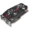
ASUS GTX 580 Matrix Platinum 1.5 GB Review
Test Setup »A Closer Look
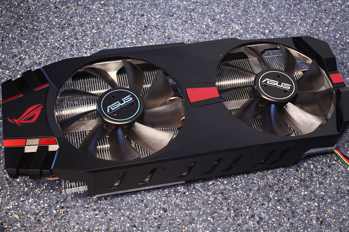
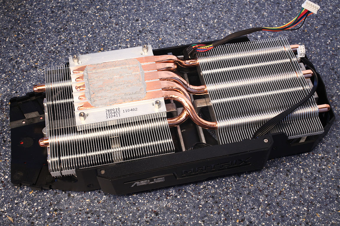
ASUS continues use of their Direct CU cooler design which uses five heatpipes that make direct contact with the GPU surface.


To cool the voltage regulation circuitry this massive metal heatsink is used. It sits in the airflow of the right side fan to keep it cool.


On the back of the card a metal plate has been installed which adds to the visual impression of the card, protects components on the back from accidential damage and acts as passive heatsink for heat moving through the PCB to the back of the card.
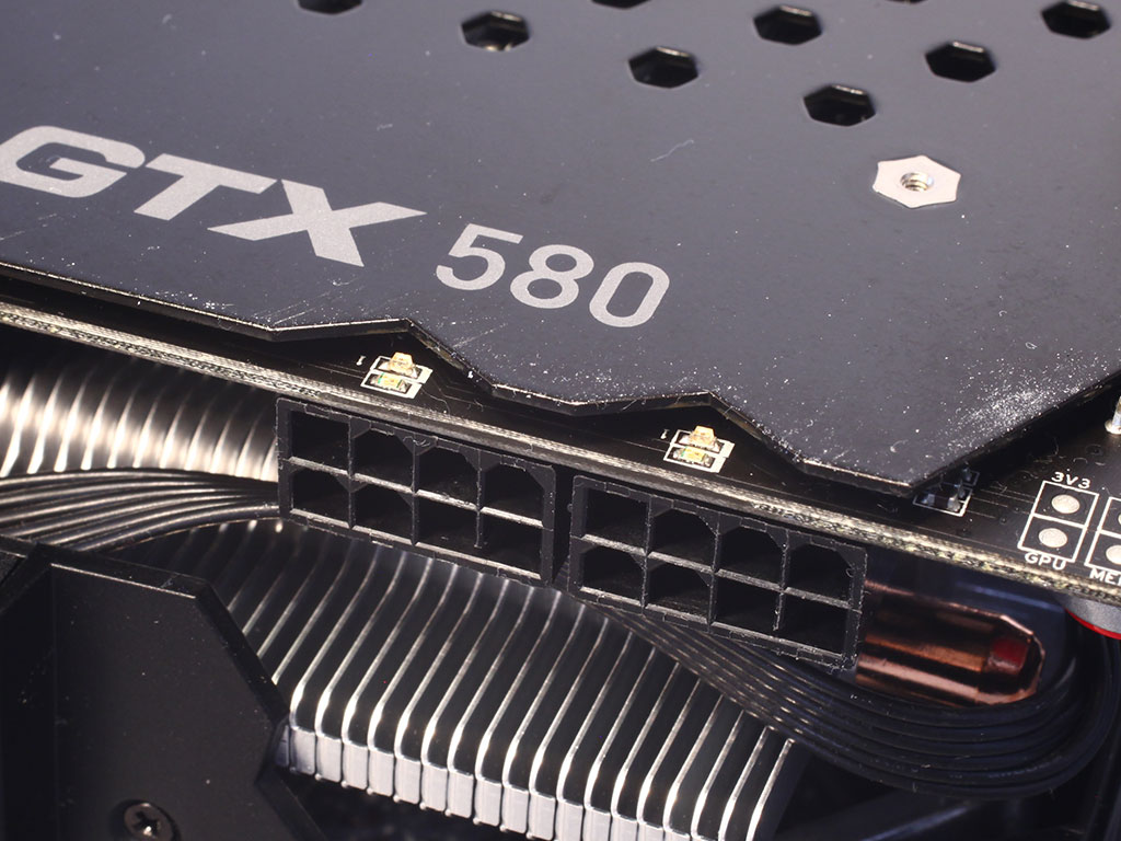
The cards has two 8-pin PCIe power connectors. This configuration is good for up to 375 W power draw.

ASUS has placed several measuring spots near the bottom right edge of the PCB. You can measure six GPU voltages here - very nice.
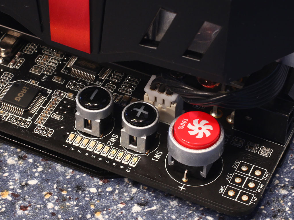

The big red button you see in the picture above sets fan speed to 100% when pressed. Once you press it again, the card returns to normal auto-controlled fan speeds. The plus and minus buttons next to the red button are used to change the GPU operating voltage. An offset of up to 12.5 mV can be applied to the whole voltage regulation circuitry, on top of any software voltage settings. All three buttons work fully in hardware - no software required.

In case your overclocking adventures are too optimistic, or you mess up a BIOS flash, pressing this button will return the card to default frequencies and the default BIOS, so you can restore operation easily.

The solderpads shown above can be bridged by solder or a 0 Ohm resistor to activate advanced functionality. "Disable OCP" disabled overheat protection and removes overcurrent protection for LN2 overclocking. "FBDDO" is used to increase memory voltage, "PEXVDD" increases PLL voltage and "Power PWM Freq" doubles the voltage regulator clock frequency from 250 kHz to 500 kHz.
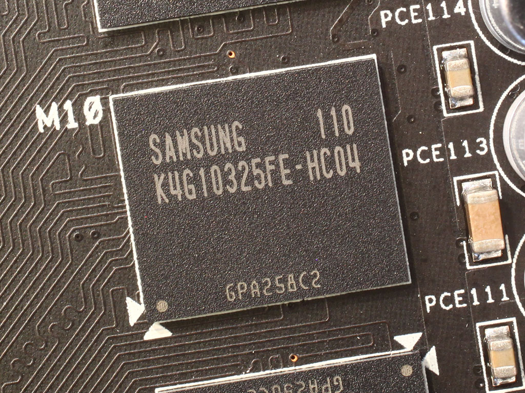
The GDDR5 memory chips are made by Samsung, and carry the model number K4G10325FE-HC04. They are specified to run at 1250MHz (5000 MHz GDDR5 effective).

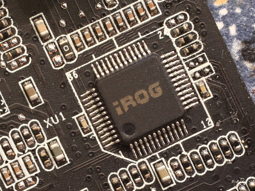
ASUS has rebranded the voltage controller on their card to show "SHE: Super Hybrid Engine". It looks like a model from uPI with software voltage control. A second chip called "iROG" is also placed on the board, it seems to control the three button and the glowing Matrix current load indicator.

NVIDIA's GeForce 110 graphics processor is made on a 40 nm process at TSMC Taiwan. It uses approximately 3.0 billion transistors which is 200 million less than the GF100. Please note that the silvery metal surface you see is the heatspreader of the GPU. According to NVIDIA, the die size of the GF110 graphics processor is 520 mm².
Apr 18th, 2024 08:38 EDT
change timezone
Latest GPU Drivers
New Forum Posts
- What's your latest tech purchase? (20256)
- [Official] Meta Quest 3 (44)
- Realtek Modded Audio Driver for Windows 10/11 - Only for HDAUDIO (5678)
- Will a RTX 4070 TI super bottleneck a Ryzen 9 7950X3D? (33)
- Which air cooler for a ryzen 9 5900x (157)
- What are you playing? (20454)
- Unlocked Realtek HD Audio Drivers for Windows 11 (Dolby Digital Live/DTS Interactive) (152)
- The TPU UK Clubhouse (24726)
- Gigabyte gpu model differences? (33)
- DDR5 RAM Speeds and the future (25)
Popular Reviews
- Horizon Forbidden West Performance Benchmark Review - 30 GPUs Tested
- PowerColor Radeon RX 7900 GRE Hellhound Review
- Fractal Design Terra Review
- Corsair 2000D Airflow Review
- Minisforum EliteMini UM780 XTX (AMD Ryzen 7 7840HS) Review
- Creative Pebble X Plus Review
- FiiO KB3 HiFi Mechanical Keyboard Review - Integrated DAC/Amp!
- ASUS GeForce RTX 4090 STRIX OC Review
- NVIDIA GeForce RTX 4090 Founders Edition Review - Impressive Performance
- ASUS GeForce RTX 4090 Matrix Platinum Review - The RTX 4090 Ti
Controversial News Posts
- Sony PlayStation 5 Pro Specifications Confirmed, Console Arrives Before Holidays (106)
- NVIDIA Points Intel Raptor Lake CPU Users to Get Help from Intel Amid System Instability Issues (102)
- US Government Wants Nuclear Plants to Offload AI Data Center Expansion (98)
- Windows 10 Security Updates to Cost $61 After 2025, $427 by 2028 (82)
- Developers of Outpost Infinity Siege Recommend Underclocking i9-13900K and i9-14900K for Stability on Machines with RTX 4090 (82)
- TechPowerUp Hiring: Reviewers Wanted for Motherboards, Laptops, Gaming Handhelds and Prebuilt Desktops (71)
- Intel Realizes the Only Way to Save x86 is to Democratize it, Reopens x86 IP Licensing (70)
- AMD Zen 5 Execution Engine Leaked, Features True 512-bit FPU (63)