 65
65
ASUS Maximus V Gene Intel Z77 Express LGA 1155 Review
BIOS Walkthrough »The Board - A Closer Look


When first firing up the board, you've got a couple of options on how to do so, thanks to the on-board buttons found by the board edges. On the bottom edge is the POWER and RESET buttons in the first image above, while the little red "GO" button, in the second image, is just above the 24-pin power connector. That "GO" button can be used to ensure a stable boot no matter what memory is installed, or can initiate an OC profile when the board is running, the settings to which are available for modification inside the BIOS.


The socketed BIOS chip itself is also on the board's bottom edge, while just below the SATA ports I found a dual-DIGIT POST display. Right next to the 24-pin power plug is a series of LEDs that visually indicate where in the POST process the board is, which together help to quickly pin-point boot problems.


The CPU VRM design is an 8+4 design, with eight phases for the CPU proper, and four for the iGPU portion. There are six input drivers total, each of which powers two phases. The DIMM VRM is of a similar design, with a single input driving dual output phases, shown in the second image above.


The system agent is also powered like the other CPU phases, shown in the first image above, with a single input driver and dual output phases, to help push memory speeds to the max. The PCH power delivery, found between the PCIe slots, also apears to have a dual output, with dual chokes seen close by.


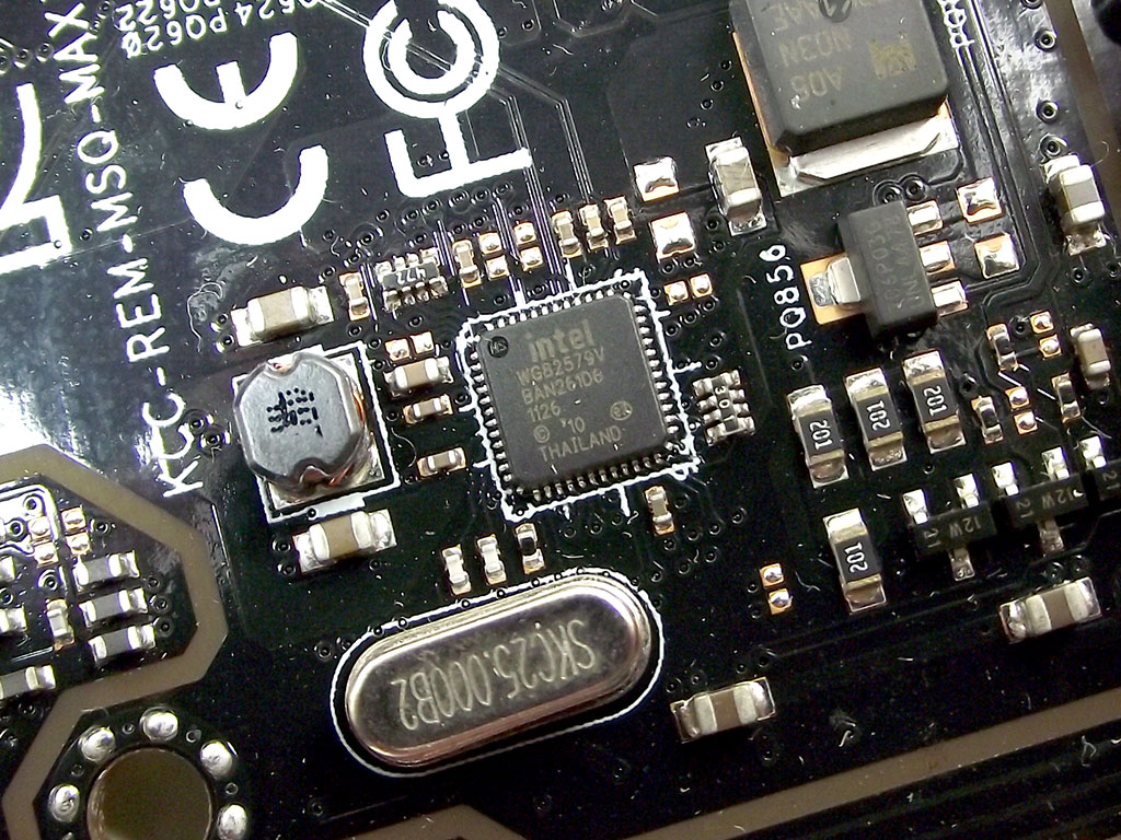
To monitor all that functionality, I found direct measure points on the board's right edge by the DIMM slots, as well as a Nuvoton NCT67790 Super I/O, for monitoring duties inside the OS. LAN connectivity is provided by an Intel WG82578V GbE controller, found on the board's left edge.


ASMedia provides both the secondary SATA 6 Gb/s ASM1061 controller, as well as the ASM1042 USB 3.0 controller
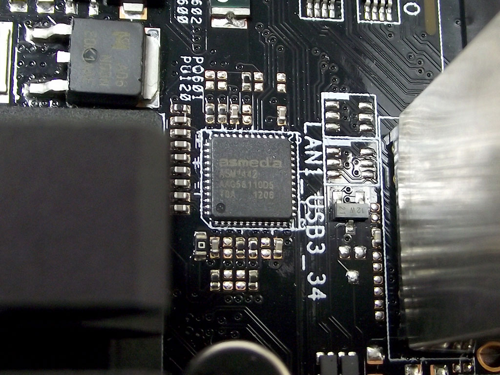

The ASM1442 TMDS link and ASM1480 PCIe switches are also provided by ASMedia.
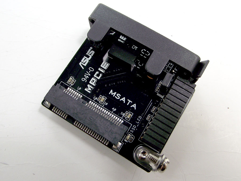

the mPCIe add-on card, shown in the pictures above, is a neat little innovation that adds a mPCIe port on one side, and a mSATA port on the other. With space as limited as it is on a mATX product, this allows all the features that the Intel Z77 Express platform offers, although seperate purchase of components to fit into the card is necessary.


Fortunately, I've got such devices on-hand, and installed them as shown in the above pictures. For an mSATA drive, I used an OCZ Nocti 60 GB drive, and for mPCIe, I installed an Atheros-based WiFi/Bluetooth combo unit.

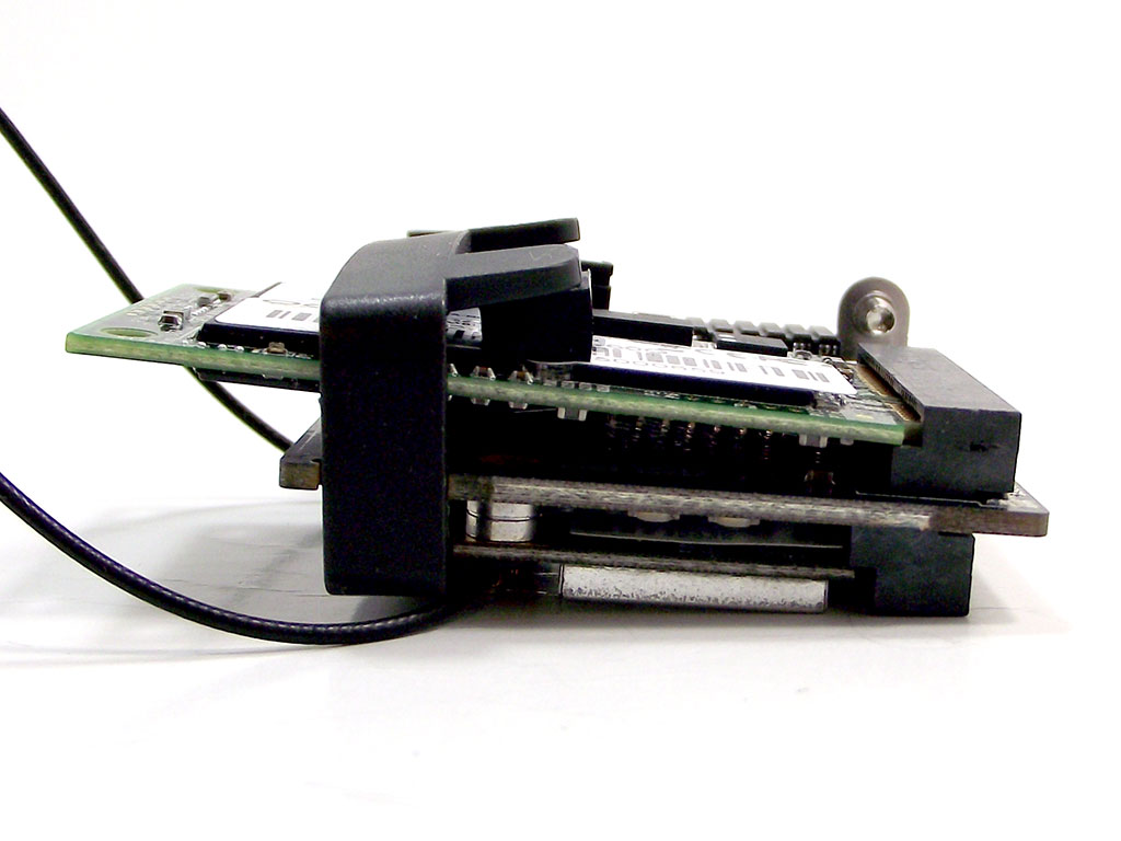
As you can see in the pictures, there is a black plastic clip that holds the mSATA drive in place, using a single rubber pad on the card's PCB surface and two additional rubber pads on the bracket itself. To me, the pad on the PCB itself is too thick, and causes the OCZ mSATA drive to sit at an angle to the card's surface, and then places additional force on the black plastic bracket making it bow out, and causing the rubber pads on the bracket to pull away from the adhesive used to attach them. I'm not very fond of this mechanism, and do not place much faith on it being very secure and holding the mSATA drive in place in the long run. The mPCIe side, on the other hand, attaches the card in place with two screws that are found already installed in the mounting posts. There is very little excess room here, and I had to twist the antenna wires of the Atheros card out of the way before I could secure the mSATA drive properly.


Anyway, the card itself attaches to the board's surface at the top of the rear I/O, via a 25-pin header. Once installed, it attaches securely in place via a single screw, and is oriented so that if you use a mPCIe wireless card, the WiFi card is facing the top where the holes in the rear I/O cover for antennas are.

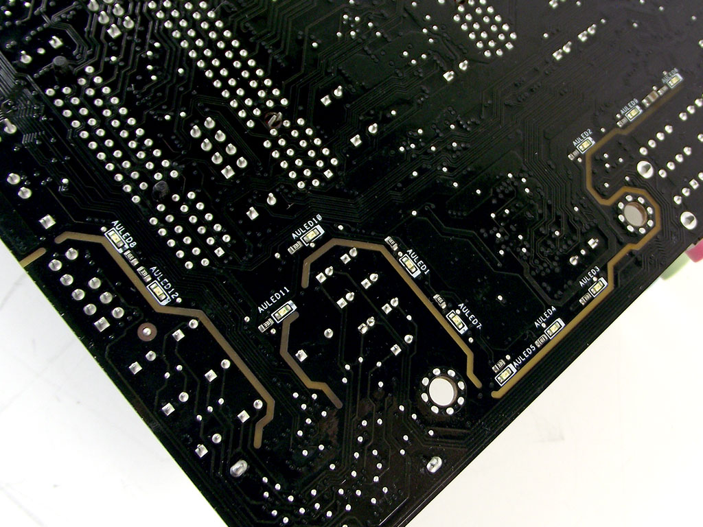

The audio portion of the ASUS Maximus V Gene is quite the thing, with the actual audio CODEC covered by a metal shield, to prevent electrical interference from other parts. The yellowish line you see in the second picture above is a bare area on the PCB that goes through all layers, and that ensures the audio portion is islolated from the rest of the board, with only a few SMDs and the audio CODEC itself connected to the rest of the board electrically. There are also a bunch of LEDs around that line, that light up red when the board is powered up, and can they be turned off in the BIOS.


As you can see in the two images above, the LEDs are pretty bright, so much so that they shine through the PCB itself, illuminating the line of isolation. This bit draws attention to this innovation, as well as offering a bit of "bling", great for windowed cases.


The coolers, as I mentioned earlier, are finished with flat black anodizing, and both the VRM and PCH cooler are pretty thick, for more-than-ample cooling ability. Looking at the contact areas once I removed the coolers, I found perfect contact impressions on the VRM cooler with all of the MOSFETs, the input drivers, and the controller itself. The PCH cooler uses that same pink gummy TIM we've seen often, which I think is provided by HoneyWell. A couple of pieces stuck to the PCH's smooth silicon surface, and pulled away when I removed the cooler, a good sign that the contact made is pretty secure.
Apr 25th, 2024 04:04 EDT
change timezone
Latest GPU Drivers
New Forum Posts
- Alphacool CORE 1 CPU block - bulging with danger of splitting? (4)
- The TPU UK Clubhouse (24786)
- Github comments used to push malware via Microsoft repo urls (3)
- Bizarre Throttlestop issue (5)
- Core i5-6300U (13)
- GTX 1070 Ti - TDP Issues - Always Power Throttling (5)
- What phone you use as your daily driver? And, a discussion of them. (1471)
- (Anti) SFF fun house (349)
- What's your latest tech purchase? (20337)
- The Official Linux/Unix Desktop Screenshots Megathread (694)
Popular Reviews
- Fractal Design Terra Review
- Thermalright Phantom Spirit 120 EVO Review
- Corsair 2000D Airflow Review
- Minisforum EliteMini UM780 XTX (AMD Ryzen 7 7840HS) Review
- ASUS GeForce RTX 4090 STRIX OC Review
- NVIDIA GeForce RTX 4090 Founders Edition Review - Impressive Performance
- ASUS GeForce RTX 4090 Matrix Platinum Review - The RTX 4090 Ti
- MSI GeForce RTX 4090 Suprim X Review
- MSI GeForce RTX 4090 Gaming X Trio Review
- Gigabyte GeForce RTX 4090 Gaming OC Review
Controversial News Posts
- Sony PlayStation 5 Pro Specifications Confirmed, Console Arrives Before Holidays (116)
- NVIDIA Points Intel Raptor Lake CPU Users to Get Help from Intel Amid System Instability Issues (106)
- AMD "Strix Halo" Zen 5 Mobile Processor Pictured: Chiplet-based, Uses 256-bit LPDDR5X (101)
- US Government Wants Nuclear Plants to Offload AI Data Center Expansion (98)
- Windows 10 Security Updates to Cost $61 After 2025, $427 by 2028 (84)
- Developers of Outpost Infinity Siege Recommend Underclocking i9-13900K and i9-14900K for Stability on Machines with RTX 4090 (84)
- TechPowerUp Hiring: Reviewers Wanted for Motherboards, Laptops, Gaming Handhelds and Prebuilt Desktops (78)
- AMD's RDNA 4 GPUs Could Stick with 18 Gbps GDDR6 Memory (75)