 141
141
ASUS Radeon R9 Fury STRIX 4 GB Review
Packaging & Contents »Architecture
At the heart of the Radeon R9 Fury is the most talked about GPU of the season, codenamed "Fiji." It is a multi-chip module out of three important components—the GPU die itself, built on TSMC's 28 nm process, a specially designed silicon substrate layer that seats and connects the GPU die with the HBM memory stacks called interposer and built by UMC on its 65 nm process, and four 1 GB HBM stacks made by SK Hynix on a 20 nm-class node. AMD had technical assistance from some of the industry's brightest VLSI teams, including from UMC, Amkor Technology, ASE Group, and SK Hynix.Let's begin with the GPU die itself. It features a familiar component hierarchy to the previous-generation "Hawaii" silicon. The Graphics CoreNext stream processors, however, are of a newer generation, GCN 1.2, which made its debut with the "Tonga" silicon that powers the Radeon R9 380 and R9 285. As we mentioned before, AMD created the R9 Fury by disabling a few components on the "Fiji" silicon. Those disabled components are shaded red in the architecture diagram below.
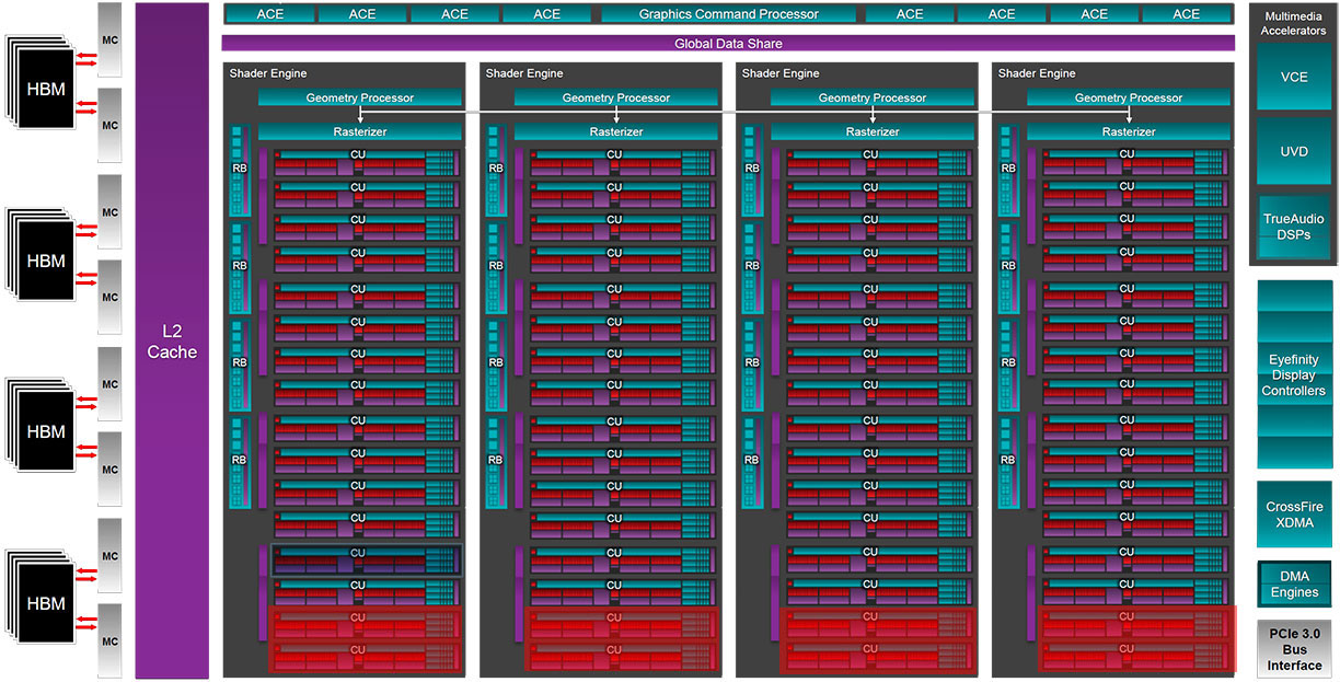
The GPU die features four shader engines, just like "Hawaii," but the compute unit (CU) count per shader engine has been increased to 14 from the 11 on "Hawaii." Each CU packs 64 stream processors, so there are 896 stream processors per engine and 3,584 on the chip in total. There are 16 render back-ends, which is the same as with "Hawaii," so the ROP count is the same at 64. The higher CU count, however, means that the TMU count is at 224 instead of the 176 on "Hawaii." The biggest change, however, is the 4096-bit wide HBM interface that wires out to four 8 Gigabit HBM stacks. AMD carved the R9 Fury out of the "Fiji" silicon by enabling 56 of the 64 compute units.
AMD didn't announce any changes to the ancillaries—the multimedia engine, XDMA CrossFire (no bridge cables required), display controllers with support for DisplayPort 1.2a and HDMI 1.4a, and PCI-Express gen 3.0 x16 host interface remain the same as on "Hawaii." There is one notable change, though, since the reference design card lacks DVI connectors. It features a HDMI and three DP 1.2a ports. All ports are on the first slot elevation, making this card truly single-slot capable with aftermarket liquid-cooling blocks (the piggybacked DVI connector that extends into the second slot denies NVIDIA cards this cool feature unless you're skillful enough to solder out the DVI connector without accidentally shorting any pins).
High Bandwidth Memory and Interposer
With Windows 10 and its companion DirectX 12 API on the horizon and high display resolutions such as 1440p and 4K Ultra HD getting increasingly more affordable—1440p displays start at $250 and 4K starts at $400 if you know where to look—the demands on video memory to catch up have never been higher. GDDR5 served the industry well since its debut in 2008. It has driven five generations of GPUs since, but is approaching its design limitation for performance upscaling through clock-speed increases.

For any memory standard (including HBM), memory speed/bandwidth and power draw don't scale linearly. Beyond a point, the equation tapers too much in favor of power requirements, and so, an increasingly disproportionate amount of power is required to achieve higher clocks. This is what necessitates a new memory standard. HBM is just starting out on that same curve, and has, hence, much better energy efficiency than GDDR5. HBM trades frequency for bus-width and offers vertical stacking of DRAM dies. This generation of HBM allows vertical stacking of up to four DRAM dies, with a fifth logic die holding the PHY and connections of the stack.
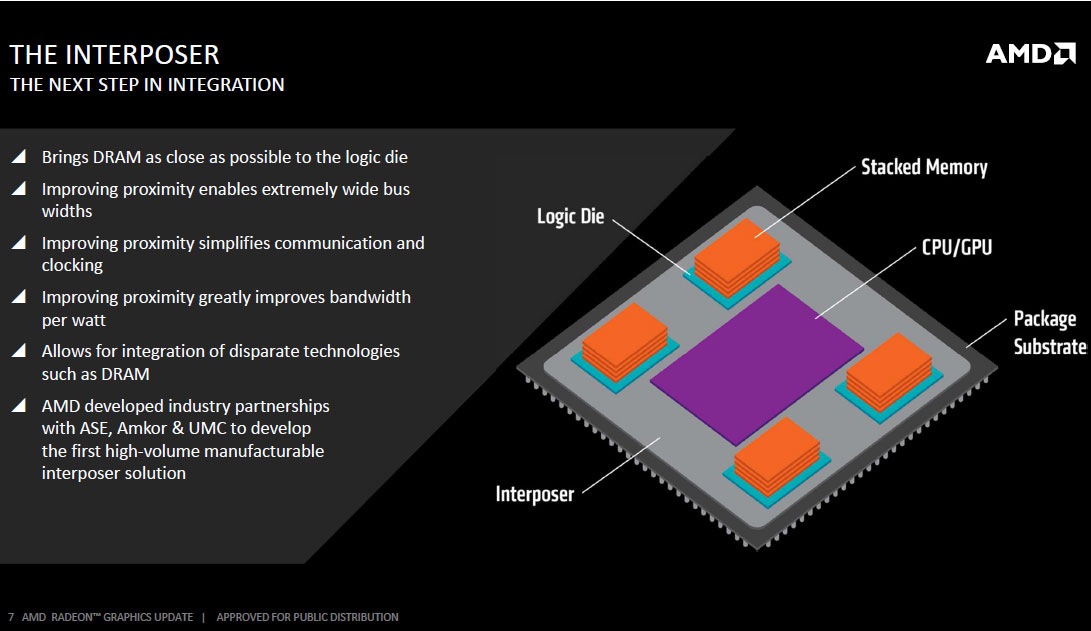
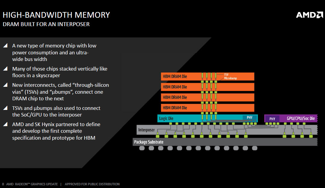
The Fiji package features four 8 Gb HBM stacks, each with 1,024-bit wide memory bus. Since such a wide bus per stack would take up an obscene number of pins on a standalone memory chip package, AMD decided to integrate it into the GPU package, using a specially designed substrate called the interposer to deal with the wiring problem.
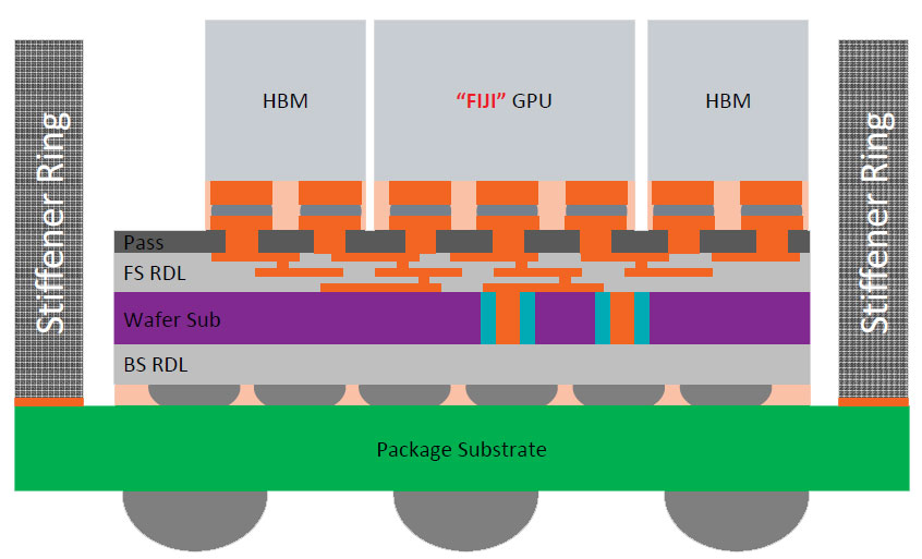
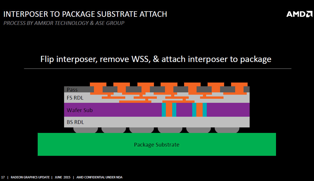
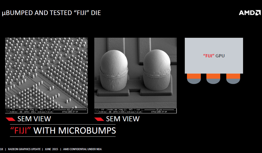
The interposer is essentially a very large silicon die that acts as a substrate for other dies. There's no number crunching or storage happening here as there is just a vast network of microscopic wires running between the HBM stacks and the GPU die. The interposer is built on a 65 nanometer silicon fab node. It may not sound like much in the 20 nm-class era, but compared to conventional fiberglass PCB wiring, wires on the 65 nm node are infinitesimally smaller, as are bumps, points of contact between two dies or between a die and a substrate. AMD innovated microscopic bumps specifically for contact between the GPU die and the interposer because wiring between the GPU and the memory is just so dense.

The interposer has microscopic bumps on the side that faces toward the GPU die and HBM stacks and conventional bumps, also on the side, that face toward the main fiberglass substrate of the GPU package. With the memory moved to the GPU package, and more importantly, the most sensitive wiring of the video card (that between the memory and GPU) moved to the GPU package, there's not much action on the PCB. The pins on the package are for power, system bus, and display I/O, which gives AMD greater quality control.


Another major benefit of moving the memory to the GPU package, however, is the savings in PCB real-estate. Sure, the package in itself is bigger than "Hawaii" or any GPU ever made, but since there are no memory chips surrounding it, all that's left on the video card's PCB are the GPU package, VRM, and display I/O. This allows AMD to create some extremely compact products. Unlike the reference R9 Fury X, the ASUS R9 Fury STRIX, however, offers a conventionally sized PCB. Despite the meaty VRM, you can still see large empty areas on the PCB.
Apr 19th, 2024 20:33 EDT
change timezone
Latest GPU Drivers
New Forum Posts
- Official Board Game Discussion (0)
- GTX 1060 6GB ASUS GPU Shuts Down after 5min of Gaming (1)
- AMD RX 7000 series GPU Owners' Club (1068)
- I just succesfully baked DDR4 (69)
- I9 13890HX undervolting Suggestions (4)
- Undervolting Dell XPS 14 9440 is it possible? (7)
- Share your AIDA 64 cache and memory benchmark here (2884)
- Roccat Kone AIMO has developed a double left click, when I click it once. Any fix out there? (34)
- The TPU UK Clubhouse (24738)
- XFX RX580 stock Bios (7)
Popular Reviews
- Horizon Forbidden West Performance Benchmark Review - 30 GPUs Tested
- Fractal Design Terra Review
- Corsair 2000D Airflow Review
- Thermalright Phantom Spirit 120 EVO Review
- Minisforum EliteMini UM780 XTX (AMD Ryzen 7 7840HS) Review
- Creative Pebble X Plus Review
- FiiO KB3 HiFi Mechanical Keyboard Review - Integrated DAC/Amp!
- ASUS GeForce RTX 4090 STRIX OC Review
- NVIDIA GeForce RTX 4090 Founders Edition Review - Impressive Performance
- ASUS GeForce RTX 4090 Matrix Platinum Review - The RTX 4090 Ti
Controversial News Posts
- Sony PlayStation 5 Pro Specifications Confirmed, Console Arrives Before Holidays (111)
- NVIDIA Points Intel Raptor Lake CPU Users to Get Help from Intel Amid System Instability Issues (102)
- US Government Wants Nuclear Plants to Offload AI Data Center Expansion (98)
- AMD "Strix Halo" Zen 5 Mobile Processor Pictured: Chiplet-based, Uses 256-bit LPDDR5X (84)
- Windows 10 Security Updates to Cost $61 After 2025, $427 by 2028 (82)
- Developers of Outpost Infinity Siege Recommend Underclocking i9-13900K and i9-14900K for Stability on Machines with RTX 4090 (82)
- TechPowerUp Hiring: Reviewers Wanted for Motherboards, Laptops, Gaming Handhelds and Prebuilt Desktops (72)
- Intel Realizes the Only Way to Save x86 is to Democratize it, Reopens x86 IP Licensing (70)