 307
307
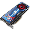
HIS Radeon HD 6970 2 GB Review
Packaging & Contents »Architecture

Cayman, named after the lovely Cayman islands in the Caribbean, is AMD's new high-end GPU. It succeeds Cypress, on which were based Radeon HD 5800 series and the dual-GPU HD 5970. Cayman is built on existing 40 nm process at TSMC. Apart from the processor most of the components inside are the same as the ones found in the previous generation GPUs, except that the hierarchy of components is changed to add a degree of parallelism that goes a step ahead of even Barts. The SIMD cores are completely restructured, too.

With Cypress, there was only one graphics engine (that which computes preliminary data and instructions, and passes them on for low-level processing to the SIMD cores), and one dispatch processor that funneled data and instructions down to the two SIMD engine blocks. Barts introduced a degree of parallelism by giving each SIMD engine block its own dispatch processor, instruction and constant caches. Cayman is taking that a step further, by splitting even the graphics engines between the two SIMD engine blocks. This gives dedicated rasterizers, geometry assemblers to each block, but more importantly, doubles the number of tessellation units, with each graphics engine having one.


As mentioned earlier, AMD brought about a radical change in the stream processor design. Compared to the older VLIW5 design in which an SIMD core consisted of four simple and one complex stream processors with some common resources, the new design, dubbed VLIW4, combines four equally-capable complex stream processors, with two of the four getting special functions. Overall, with a stream processor count of 1536, the Radeon HD 6970 clocked at 880 MHz, is able to churn out a single-precision floating point (IEEE754-SP) performance of 2.7 TFLOPs, and double-precision performance (IEEE754-DP) of 675 GFLOPs. The VLIW4 architecture, hence is aimed to increase performance per mm² of die-area. The render back-ends, have also been redesigned to facilitate 2 times faster 16-bit integer and 32-bit floating-point operations.
In a nutshell, the Cayman die measures 389 mm², holding 2.64 billion transistors. It is built on the 40 nm TSMC process. It has 24 SIMD engines spread across two SIMD engine blocks. There are 1536 stream processors in all. There are 96 texture memory units (TMUs), and 32 raster operation processors (ROPs). New, faster memory controllers allow use of new 5.5 Gbps memory chips. The memory bus width is 256-bit, with which the GPU connects to eight 2 Gbit memory chips to archive 2 GB of total memory.
Apr 23rd, 2024 15:47 EDT
change timezone
Latest GPU Drivers
New Forum Posts
- Aida64 cache mem OC (0)
- windows 11 (4)
- Which new games will you be buying? (299)
- Meta Horizon OS (5)
- No POST, and no display (6)
- need help with motherboard/ ram compability certainty (5)
- My computer setup - Request for opinions (11)
- EK seems to be having major issues (26)
- DeepCool AIO LS720 RGB NOT WORKING HELP! (0)
- Is there a technical reason that Windows 11 doesn't have built into it battery charge limitation? (36)
Popular Reviews
- Horizon Forbidden West Performance Benchmark Review - 30 GPUs Tested
- Fractal Design Terra Review
- Corsair 2000D Airflow Review
- Thermalright Phantom Spirit 120 EVO Review
- Minisforum EliteMini UM780 XTX (AMD Ryzen 7 7840HS) Review
- ASUS GeForce RTX 4090 STRIX OC Review
- NVIDIA GeForce RTX 4090 Founders Edition Review - Impressive Performance
- ASUS GeForce RTX 4090 Matrix Platinum Review - The RTX 4090 Ti
- Creative Pebble X Plus Review
- MSI GeForce RTX 4090 Gaming X Trio Review
Controversial News Posts
- Sony PlayStation 5 Pro Specifications Confirmed, Console Arrives Before Holidays (116)
- NVIDIA Points Intel Raptor Lake CPU Users to Get Help from Intel Amid System Instability Issues (105)
- AMD "Strix Halo" Zen 5 Mobile Processor Pictured: Chiplet-based, Uses 256-bit LPDDR5X (101)
- US Government Wants Nuclear Plants to Offload AI Data Center Expansion (98)
- Windows 10 Security Updates to Cost $61 After 2025, $427 by 2028 (84)
- Developers of Outpost Infinity Siege Recommend Underclocking i9-13900K and i9-14900K for Stability on Machines with RTX 4090 (84)
- TechPowerUp Hiring: Reviewers Wanted for Motherboards, Laptops, Gaming Handhelds and Prebuilt Desktops (74)
- Intel Realizes the Only Way to Save x86 is to Democratize it, Reopens x86 IP Licensing (70)