 36
36
Intel Core i3-8350K 4.0 GHz Review
Test Setup »Architecture
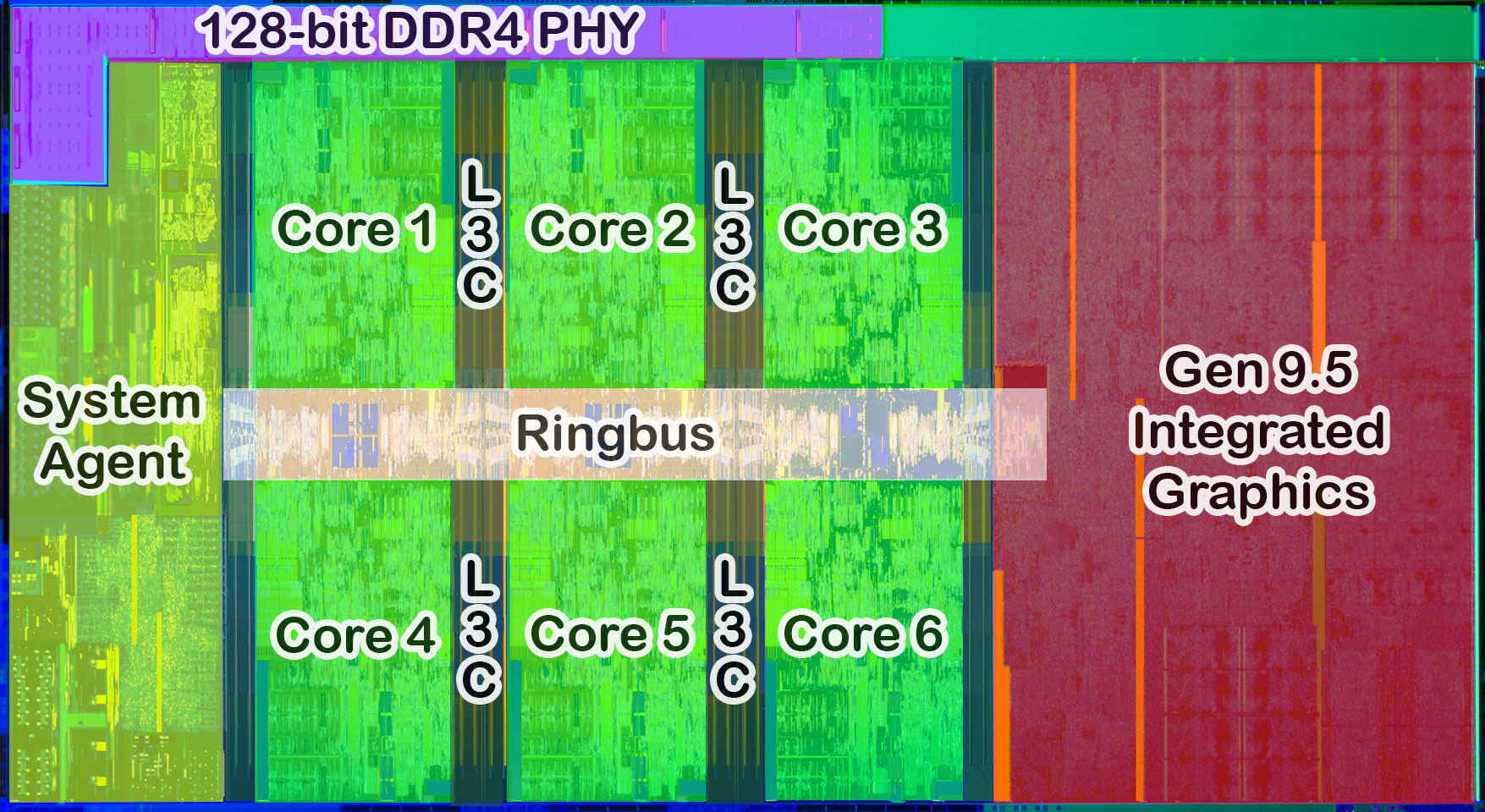
The 8th generation Intel Core processors are based on the "Coffee Lake" micro-architecture. The CPU circuit design is essentially the same as "Skylake," but the silicon is built on Intel's third iteration of the 14 nanometer silicon fab process, which the company refers to as 14 nm++. This node improves the ability for the chipmaker to dial up clock speeds at minimal power/thermal cost. While the quad-core "Kaby Lake" silicon was "Skylake" built on a refined 14 nm+ process, the six-core "Coffee Lake" silicon is a new design with a die-area of 150 mm².The "Coffee Lake" silicon physically features six CPU cores with 256 KB of dedicated L2 cache per core and 12 MB of shared L3 cache. On the Core i5 "Coffee Lake" series, the L3 cache is limited to 9 MB, which still keeps up with the concept of 1.5 MB/core L3 cache for Core i5 SKUs. The integrated Gen 9.5 graphics core is physically carried over from the "Kaby Lake" die, but is bolstered by higher clocks and an enhanced driver, which lets Intel brand it as the "Intel UHD Graphics 600 series." Internal communication is handled by a "ring bus" and not the mesh-interconnect Intel deployed on its new Core X "Skylake-X" processors.

The system agent (the integrated Northbridge) also appears to be carried over from the "Kaby Lake" die, with its dual-channel DDR4 memory interface. There are minor improvements, such as the standard DDR4 memory clock being upped to DDR4-2666 on the Core i7 and Core i5 SKUs, and DDR4-2400 on the Core i3 SKUs. The IMC supports XMP 2.0 profiles. The processor only puts out 16 PCI-Express gen 3.0 lanes meant for PEG (PCI-Express discrete graphics). It talks to the motherboard chipset over the DMI 3.0 chipset bus, with a 32 Gbps-per-direction bandwidth.
The "Coffee Lake" CPU core is of the same exact design as Skylake and Kaby Lake, which dates back to 2015. Compared to the Haswell/Broadwell core, it features an improved front-end with a 25% fatter 5 µOP pipeline, a 50% wider allocation queue depth; an improved branch-prediction unit, and a wider instruction window. The execution stage features a slightly bigger re-order buffer, a bigger integer register file, an improved on-chip memory system. All of these contributed to a 5-10 percent IPC increase over "Haswell" to "Skylake" clock-for-clock.

Between "Skylake" and "Coffee Lake," Intel turned its R&D efforts toward refining the 14 nm process. It met with success on "Kaby Lake," and owing to its significantly higher clock speeds, "Kaby Lake" was able to provide higher performance than "Skylake." With "Coffee Lake," the nominal clock speeds look low, but Turbo Boost frequencies are higher than "Kaby Lake," and refinements in the process allow the chip to sustain elevated boost clock states better. As we mentioned throughout the introduction, the design focus of these chips is to increase core counts across the board in order to better compete with AMD Ryzen.
The Gen 9.5 integrated graphics core takes up nearly a third of the die area. Since it's of the same core configuration as the one on the "Kaby Lake" silicon, it still features 24 execution units in the GT2 trim (featured on the i7-8700K). Higher clocks, coupled with some driver magic, let Intel brand it "UHD Graphics." Don't expect to play PUBG at 4K on this; the "UHD" moniker only indicates that the IGP can handle 4K Ultra HD displays, features modern connectivity options such as DP 1.4 and HDMI 2.0, and can playback 4K video in new formats with 10-bpc color and HDR10/Dolby Vision standards.
The Z370 Platform
Intel is launching its first Core "Coffee Lake" processors alongside the Z370 Express chipset. Less expensive B360 Express and H310 Express models will be introduced in Q1-2018. The Z370 Express chipset, which succeeds the Z270 Express, appears to carry over the same platform feature set. It wouldn't surprise us if the Z370 turns out to be a re-brand of the Z270; however, we have no way of telling right now. Perhaps we will deal with this question in our upcoming motherboard reviews. As we mentioned on the previous page, 8th generation Core processors won't work on 100-series/200-series chipset motherboards.
This chipset compensates for the narrow 16-lane PCI-Express root complex of the CPU by putting out 24 general-purpose PCI-Express gen 3.0 lanes. That's a good enough lane budget for up to three 32 Gbps NVMe devices (M.2 or U.2), the x4 and x1 PCIe slots, and even bandwidth-hungry onboard devices such as Thunderbolt 3 controllers, additional USB 3.1 gen 2.0 controllers, 10 GbE network controllers, etc. The integrated SATA controller puts out six SATA 6 Gbps ports with RAID support; the chipset also puts out two 10 Gbps USB 3.1 gen 2.0 ports, and up to eight 5 Gbps USB 3.1 gen 1.0 ports, besides a number of USB 2.0 ports.
Apr 23rd, 2024 18:47 EDT
change timezone
Latest GPU Drivers
New Forum Posts
- What's your latest tech purchase? (20307)
- My computer setup - Request for opinions (12)
- Show us your collections thread!! (282)
- Realtek Modded Audio Driver for Windows 10/11 - Only for HDAUDIO (5687)
- need help with motherboard/ ram compability certainty (11)
- What phone you use as your daily driver? And, a discussion of them. (1454)
- Is there a technical reason that Windows 11 doesn't have built into it battery charge limitation? (37)
- ThrottleStop 9.6 Voltage won't change (1)
- FINAL FANTASY XIV: Dawntrail Official Benchmark (71)
- CPB Enabled Boot Loop (8)
Popular Reviews
- Horizon Forbidden West Performance Benchmark Review - 30 GPUs Tested
- Fractal Design Terra Review
- Corsair 2000D Airflow Review
- Thermalright Phantom Spirit 120 EVO Review
- Minisforum EliteMini UM780 XTX (AMD Ryzen 7 7840HS) Review
- ASUS GeForce RTX 4090 STRIX OC Review
- NVIDIA GeForce RTX 4090 Founders Edition Review - Impressive Performance
- ASUS GeForce RTX 4090 Matrix Platinum Review - The RTX 4090 Ti
- Creative Pebble X Plus Review
- MSI GeForce RTX 4090 Gaming X Trio Review
Controversial News Posts
- Sony PlayStation 5 Pro Specifications Confirmed, Console Arrives Before Holidays (116)
- NVIDIA Points Intel Raptor Lake CPU Users to Get Help from Intel Amid System Instability Issues (106)
- AMD "Strix Halo" Zen 5 Mobile Processor Pictured: Chiplet-based, Uses 256-bit LPDDR5X (101)
- US Government Wants Nuclear Plants to Offload AI Data Center Expansion (98)
- Windows 10 Security Updates to Cost $61 After 2025, $427 by 2028 (84)
- Developers of Outpost Infinity Siege Recommend Underclocking i9-13900K and i9-14900K for Stability on Machines with RTX 4090 (84)
- TechPowerUp Hiring: Reviewers Wanted for Motherboards, Laptops, Gaming Handhelds and Prebuilt Desktops (74)
- Intel Realizes the Only Way to Save x86 is to Democratize it, Reopens x86 IP Licensing (70)