 0
0
MSI GeForce GTX 1660 Gaming X 6 GB Review
Packaging & Contents »Architecture
The GeForce GTX 1660 is based on the same 12 nm "TU116" silicon as the GTX 1660 Ti launched last month. NVIDIA has carved out the GTX 1660 by disabling two out of 24 streaming multiprocessors (SMs), and pairing the GPU with 8 Gbps GDDR5 memory instead of 12 Gbps GDDR6. Memory bus width itself is unchanged at 192-bit wide, but the switch to GDDR5 has reduced memory bandwidth by a third (192 GB/s vs. 288 GB/s). GPU clock speeds are negligibly increased if not largely the same with 1530 MHz base and 1785 MHz GPU Boost, compared to the 1500/1770 MHz of the GTX 1660 Ti.
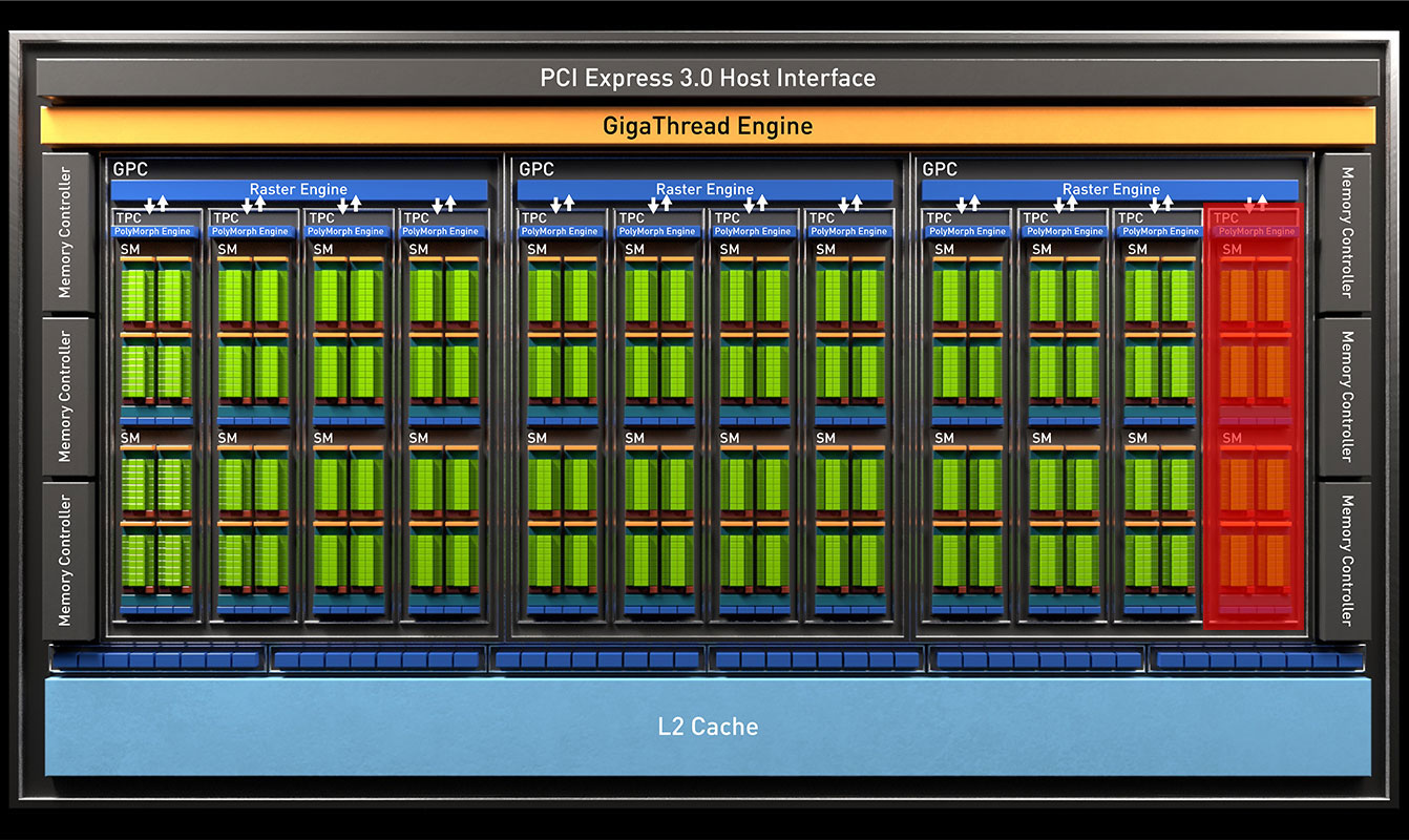
NVIDIA has significantly re-engineered the Graphics Processing Clusters (GPCs) of the silicon to lack RT cores and tensor cores. The chip's hierarchy is similar to other "Turing" GPUs. The GigaThread Engine and L2 cache are town-square for the GPU, which bind three GPCs with the chip's PCI-Express 3.0 x16 host and 192-bit GDDR5 memory interfaces. Each GPC has four indivisible TPCs (Texture Processing Cluster) that share a Polymorph Engine between two streaming multiprocessors (SM). Each Turing SM packs 64 CUDA cores, and thus, we end up with 128 CUDA cores per TPC, 512 per GPC, and 1,536 across the silicon. On the GTX 1660, there are 22 out of 24 SMs (or 11 out of 12 TPCs) enabled, which results in 1,408 CUDA cores. This is still more than the 1,280 of the GTX 1060 6 GB, and one has to also consider the increased IPC of the "Turing" architecture.


Much of NVIDIA's CUDA core specific innovation for Turing centers on improving the architecture's concurrent-execution capabilities. This is not the same as asynchronous compute, but the two concepts aren't too far out from each other. Turing CUDA cores are designed to execute integer and floating-point instructions per clock cycle in parallel, while older architectures, such as Pascal, can only handle one kind of execution at a time. Asynchronous compute is more of a macro concept and concerns the GPU's ability to handle various graphics and compute workloads in tandem.
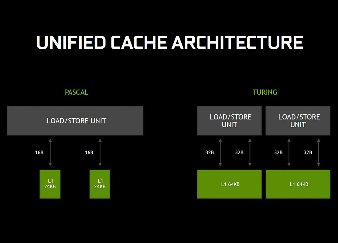
Cushioning the CUDA cores is an improved L1 cache subsystem. The L1 caches are enlarged three-fold, with a four-fold increase in load/store bandwidth. The caches are configurable on the fly as either two 32 KB partitions per SM or a unified 64 KB block per TPC. NVIDIA has also substituted tensor cores with dedicated FP16 cores per SM to execute FP16 operations. These are physically separate components to the 64 FP32 and 64 INT32 cores per SM and execute FP16 at double the speed of FP32 cores. On the RTX 2060, for example, there are no dedicated FP16 cores per SM, and the tensor cores are configured to handle FP16 ops at an enormous rate.
NVIDIA has deployed the older generation GDDR5 memory on the GTX 1660, clocked at 8 Gbps data rate compared to 12 Gbps GDDR6 on the GTX 1660 Ti. This is a massive 33 percent decrease in memory bandwidth compared to the GTX 1660 Ti and exactly the same as on the GTX 1060 6 GB. The memory amount is unchanged at 6 GB.
Features


Let's talk about the two elephants in the room first. The GTX 1660 will not give you real-time raytracing because it lacks RT cores, and won't give you DLSS for want of tensor cores. What you will get is Variable Rate Shading. The Adaptive Shading (aka variable-rate shading) feature introduced with Turing is carried over to the GTX 1660. Both its key algorithms, content-adaptive shading (CAS) and motion-adaptive shading (MAS), are available. CAS senses color or spatial coherence in scenes to minimize repetitive shading of details in pursuit of increasing detail where it matters. MAS senses high motion in a scene (e.g.: race simulators) and minimizes shading of details in favor of performance.
Apr 23rd, 2024 14:16 EDT
change timezone
Latest GPU Drivers
New Forum Posts
- Is there a technical reason that Windows 11 doesn't have built into it battery charge limitation? (35)
- My computer setup - Request for opinions (5)
- No POST, and no display (3)
- windows 11 (2)
- Cinebench crashed my PC. My Wi-Fi stopped working, and I keep getting a "Please wait" screen when I boot up my PC. (25)
- Shadow Of The Tomb Raider - CPU Performance and general game benchmark discussions (524)
- Drop fps (3)
- Embracer Group is breaking into 3 smaller companies... lol who saw this coming, what a joke (9)
- FINAL FANTASY XIV: Dawntrail Official Benchmark (69)
- Which new games will you be buying? (296)
Popular Reviews
- Horizon Forbidden West Performance Benchmark Review - 30 GPUs Tested
- Fractal Design Terra Review
- Corsair 2000D Airflow Review
- Thermalright Phantom Spirit 120 EVO Review
- Minisforum EliteMini UM780 XTX (AMD Ryzen 7 7840HS) Review
- ASUS GeForce RTX 4090 STRIX OC Review
- NVIDIA GeForce RTX 4090 Founders Edition Review - Impressive Performance
- ASUS GeForce RTX 4090 Matrix Platinum Review - The RTX 4090 Ti
- Creative Pebble X Plus Review
- MSI GeForce RTX 4090 Gaming X Trio Review
Controversial News Posts
- Sony PlayStation 5 Pro Specifications Confirmed, Console Arrives Before Holidays (116)
- NVIDIA Points Intel Raptor Lake CPU Users to Get Help from Intel Amid System Instability Issues (105)
- AMD "Strix Halo" Zen 5 Mobile Processor Pictured: Chiplet-based, Uses 256-bit LPDDR5X (101)
- US Government Wants Nuclear Plants to Offload AI Data Center Expansion (98)
- Windows 10 Security Updates to Cost $61 After 2025, $427 by 2028 (84)
- Developers of Outpost Infinity Siege Recommend Underclocking i9-13900K and i9-14900K for Stability on Machines with RTX 4090 (84)
- TechPowerUp Hiring: Reviewers Wanted for Motherboards, Laptops, Gaming Handhelds and Prebuilt Desktops (74)
- Intel Realizes the Only Way to Save x86 is to Democratize it, Reopens x86 IP Licensing (70)