Report an Error


NVIDIA GP106

GP106

GP106-300-A1
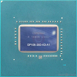
GP106-350-K3-A1

GP106-400-A1
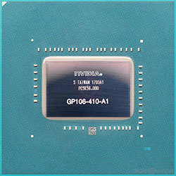
GP106-410-A1

GP106-875-A1

Fritzchens Fritz
Die Shot
Block Diagram
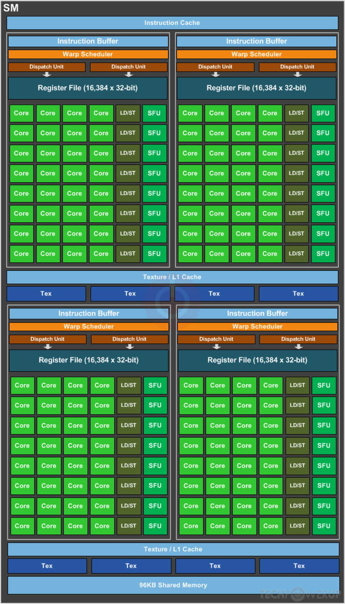
SM Diagram
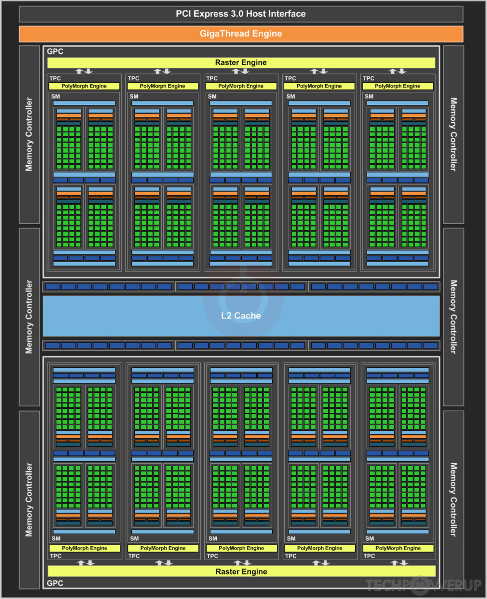
NVIDIA's GP106 GPU uses the Pascal architecture and is made using a 16 nm production process at TSMC. With a die size of 200 mm² and a transistor count of 4,400 million it is a medium-sized chip. GP106 supports DirectX 12 (Feature Level 12_1). For GPU compute applications, OpenCL version 3.0 and CUDA 6.1 can be used. It features 1280 shading units, 80 texture mapping units and 48 ROPs.
Graphics Processor
- Released
- Jul 19th, 2016
- GPU Name
- GP106
- Codename
- NV136
- Architecture
- Pascal
- Foundry
- TSMC
- Process Size
- 16 nm
- Transistors
- 4,400 million
- Density
- 22.0M / mm²
- Die Size
- 200 mm²
- Package
- BGA-2173
Graphics Features
- DirectX
- 12 (12_1)
- OpenGL
- 4.6
- OpenCL
- 3.0
- Vulkan
- 1.3
- CUDA
- 6.1
- Shader Model
- 6.7
- WDDM
- 3.1
- NVENC
- 6th Gen
- NVDEC
- 3rd Gen
- PureVideo HD
- VP8
- VDPAU
- Feature Set H
Render Config
- Shading Units
- 1280
- TMUs
- 80
- ROPs
- 48
- SM Count
- 10
- SFUs
- 320
- TPCs
- 10
- GPCs
- 2
- L1 Cache
- 48 KB per SM
- L2 Cache
- 1536 KB
- Max. TDP
- 120 W
All Pascal GPUs
NVIDIA GPU Architecture History
- 2024 Blackwell
- 2023 Hopper
- 2022-2024 Ada Lovelace
- 2020-2024 Ampere
- 2018-2022 Turing
- 2017-2020 Volta
- 2016-2021 Pascal
- 2014-2019 Maxwell 2.0
- 2014-2017 Maxwell
- 2013-2015 Kepler 2.0
- 2012-2018 Kepler
- 2010-2016 Fermi 2.0
- 2010-2013 VLIW Vec4
- 2010-2016 Fermi
- 2007-2013 Tesla 2.0
- 2006-2010 Tesla
- 2003-2013 Curie
- 2003-2005 Rankine
- 2001-2003 Kelvin
- 1999-2005 Celsius
- 1998-2000 Fahrenheit
Graphics cards using the NVIDIA GP106 GPU
| Name | Chip | Memory | Shaders | TMUs | ROPs | Base Clock | Boost Clock | Memory Clock |
|---|---|---|---|---|---|---|---|---|
| GP106-400-A1 | 6 GB | 1280 | 80 | 48 | 1506 MHz | 1709 MHz | 2002 MHz | |
| GP106-300-A1 | 3 GB | 1152 | 72 | 48 | 1506 MHz | 1708 MHz | 2002 MHz | |
| GP106-875-A1 | 5 GB | 1024 | 64 | 40 | 1076 MHz | 1480 MHz | 1752 MHz | |
| GP106-410-A1 | 6 GB | 1280 | 80 | 48 | 1506 MHz | 1709 MHz | 2257 MHz | |
| N17E-G1-A1 | 6 GB | 1280 | 80 | 48 | 1063 MHz | 1480 MHz | 2002 MHz | |
| GP106-100-A1 | 6 GB | 1280 | 80 | 48 | 1506 MHz | 1709 MHz | 2002 MHz | |
| GP106-090-A1 | 3 GB | 768 | 48 | 48 | 1354 MHz | 1531 MHz | 2002 MHz | |
| 2 GB | 768 | 48 | 32 | 1493 MHz | 1620 MHz | 1752 MHz | ||
| N17E-G1-A1 | 6 GB | 1280 | 80 | 48 | 1405 MHz | 1671 MHz | 2002 MHz | |
| GP106-350-K3-A1 | 5 GB | 1280 | 80 | 40 | 1506 MHz | 1709 MHz | 2002 MHz | |
| GP106-400-A1 | 6 GB | 1280 | 80 | 48 | 1506 MHz | 1709 MHz | 2002 MHz | |
| 5 GB | 1280 | 80 | 40 | 1000 MHz | 1493 MHz | 1251 MHz | ||
| 3.75 GB | 1152 | 72 | 32 | 1291 MHz | 1291 MHz | 1502 MHz | ||
| GP106-505-KC-A1 | 4 GB | 1152 | 72 | 32 | 1291 MHz | 1502 MHz |


GP106 GPU Notes
| NVENC: 6th Gen NVDEC: 3rd Gen PureVideo HD: VP8 VDPAU: Feature Set H Latest Drivers: Windows 7 / 8 / 8.1 (x32 / x64): GeForce Release 391.35 / 474.89 Quadro Release R390 U9 (392.37) / R440 U4 (441.66) Windows 10 / 11 (x32 / x64): GeForce Release 391.35 / Latest Quadro Release R390 U9 (392.37) / Latest |
Jun 11th, 2024 06:11 EDT
change timezone
Latest GPU Drivers
New Forum Posts
- Insyde software announces AI BIOS! (31)
- Post Your TIMESPY, PCMARK10 & FIRESTRIKE SCORES! (2019) (251)
- 9900X3D - Will AMD solve the split CCD issue (229)
- X79 and/or rampage IV OC'ing thread for those of us still left.... (2366)
- What's your latest tech purchase? (20759)
- VMware Workstation is now free for personal use (15)
- Steam Deck Owners Clubhouse (417)
- RTX 4090 Won't Undervolt via Power Limit Slider?? (6)
- Simple measurement of RADIATOR PERFORMANCE (64)
- Upgrading advice on the new AMD Processors coming out.... (29)
Popular Reviews
- Pulsar Xlite V3 Review
- Intel Lunar Lake Technical Deep Dive - So many Revolutions in One Chip
- Upcoming Hardware Launches 2024 (Updated May 2024)
- NZXT H6 Flow RGB Review
- AMD Ryzen 7 7800X3D Review - The Best Gaming CPU
- AQIRYS HYDRA 360 AIO Review
- Quick Look: Final UX2000 Wireless Noise Canceling Headphones
- Thermal Grizzly KryoSheet Review - Tested on RX 7900 XTX with 475 W
- Ghost of Tsushima Performance Benchmark Review - 35 GPUs Tested
- ASUS Radeon RX 7900 GRE TUF OC Review
Controversial News Posts
- AMD RDNA 5 a "Clean Sheet" Graphics Architecture, RDNA 4 Merely Corrects a Bug Over RDNA 3 (147)
- NVIDIA RTX 5090 "Blackwell" Founders Edition to Implement the "RTX 4090 Ti" Cinderblock Design (118)
- AMD Zen 5 Storms into Gaming Desktops with Ryzen 9000 "Granite Ridge" Processors (100)
- Biden Administration to Revive Trump-Era Tariffs on China-made GPUs and Motherboards (95)
- Nightmare Fuel for Intel: Arm CEO Predicts Arm will Take Over 50% Windows PC Market-share by 2029 (94)
- ASRock Innovates First AMD Radeon RX 7000 Graphics Card with 12V-2x6 Power Connector (94)
- AMD Ryzen 9000 Zen 5 Single Thread Performance at 5.80 GHz Found 19% Over Zen 4 (92)
- AMD Ryzen 9000 Zen 5 "Granite Ridge" Desktop Processors Launch Late-July (83)