Report an Error
SanDisk X400 1 TB
1 TB
Capacity
88SS1074
Controller
TLC
Flash
SATA 6 Gbps
Interface
2.5"
Form Factor


Tom's Hardware
PCB Front

Tom's Hardware
PCB Back

Tom's Hardware
DRAM
Tom's Hardware
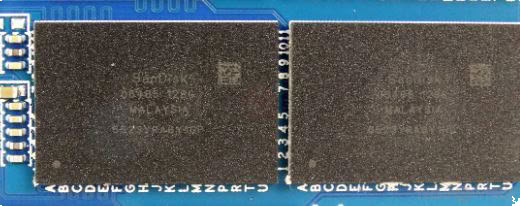
Flash

Controller

NAND Die
The SanDisk X400 was a solid-state drive in the 2.5" form factor, launched on January 5th, 2016, that is no longer in production. It was available in capacities ranging from 512 GB to 1 TB. This page reports specifications for the 1 TB variant. With the rest of the system, the SanDisk X400 interfaces using a SATA 6 Gbps connection. The SSD controller is the 88SS1074 Dean from Marvell, a DRAM cache chip is available. SanDisk has installed 64-layer TLC NAND flash on the X400, the flash chips are made by Toshiba. To improve write speeds, a pseudo-SLC cache is used, so bursts of incoming writes are soaked up more quickly, once it is full, writes complete at 275 MB/s. The X400 is rated for sequential read speeds of up to 545 MB/s and 520 MB/s write; random IOPS reach up to 95K for reads and 75K for writes.
At its launch, the SSD was priced at 240 USD. The warranty length is set to five years, which is an excellent warranty period. SanDisk guarantees an endurance rating of 320 TBW, a relatively low value compared to other SSDs.
At its launch, the SSD was priced at 240 USD. The warranty length is set to five years, which is an excellent warranty period. SanDisk guarantees an endurance rating of 320 TBW, a relatively low value compared to other SSDs.
Solid-State-Drive
| Capacity: | 1 TB (1024 GB) |
|---|---|
| Variants: | 512 GB 1 TB |
| Overprovisioning: | 70.3 GB / 7.4 % |
| Production: | End-of-life |
| Released: | Jan 5th, 2016 |
| Price at Launch: | 240 USD |
| Part Number: | SD8SB8U-1T00 |
| Market: | Consumer |
Physical
| Form Factor: | 2.5" |
|---|---|
| Interface: | SATA 6 Gbps |
| Protocol: | AHCI |
| Power Draw: |
0.07 W (Idle) 2.9 W (Avg) 4.4 W (Max) |
Controller
| Manufacturer: | Marvell |
|---|---|
| Name: | 88SS1074 Dean |
| Architecture: | ARM 32-bit ARM9/ARMv5 |
| Core Count: | Dual-Core |
| Frequency: | 400 MHz |
| Foundry: | TSMC |
| Process: | 28 nm |
| Flash Channels: | 4 @ 400 MT/s |
| Chip Enables: | 8 |
| Controller Features: | DRAM (enabled) |
NAND Flash
| Manufacturer: | Toshiba |
|---|---|
| Name: | BiCS3 |
| Rebranded: | 05478 128G (Rebranded by SanDisk) |
| Type: | TLC |
| Technology: | 64-layer |
| Speed: | 533 MT/s |
| Capacity: | 8 chips @ 1 Tbit |
| ONFI: | 3.2 |
| Toggle: | 2.0 |
| Topology: | Charge Trap |
| Process: | 19 nm |
| Dies per Chip: | 4 dies @ 256 Gbit |
| Planes per Die: | 2 |
| Decks per Die: | 2 |
| Read Time (tR): | 80 µs |
| Program Time (tProg): | 695 µs |
| Die Read Speed: | 400 MB/s |
| Die Write Speed: | 46 MB/s |
| Endurance: (up to) |
3000 P/E Cycles
(30000 in SLC Mode) |
| Page Size: | 16 KB |
| Block Size: | 768 Pages |
| Plane Size: | 1478 Blocks |
DRAM Cache
| Type: | DDR3-1866 |
|---|---|
| Name: | Micron MT41K512M8RG-107:N (D9RVX) |
| Capacity: |
1024 MB
(2x 512 MB) |
| Organization: | 4Gx8 |
Performance
| Sequential Read: | 545 MB/s |
|---|---|
| Sequential Write: | 520 MB/s |
| Random Read: | 95,000 IOPS |
| Random Write: | 75,000 IOPS |
| Endurance: | 320 TBW |
| Warranty: | 5 Years |
| MTBF: | 1.8 Million Hours |
| Drive Writes Per Day (DWPD): | 0.2 |
| SLC Write Cache: | Yes |
| Speed when Cache Exhausted: | approx. 275 MB/s |
Features
| TRIM: | Yes |
|---|---|
| SMART: | Yes |
| Power Loss Protection: | No |
| Encryption: |
|
| RGB Lighting: | No |
| PS5 Compatible: | No |
Reviews
Notes
NAND Die:Read latency: |
Jun 1st, 2024 17:55 EDT
change timezone
Latest GPU Drivers
New Forum Posts
- Your PC ATM (34594)
- How to reduce Asus mining rx470 4096 mb to 2048 mb vram? (2)
- Core counting (67)
- Dude, youre hotrodding a Dell... (0)
- Would you pay more for hardware with AI capabilities? (87)
- SSD cooling advice (0)
- 3D/Game Design Workstation (7)
- What's your latest tech purchase? (20716)
- Really interesting new Cycle HUB design. (4)
- PC Game Retro Reviews (30)
Popular Reviews
- ID-Cooling FX360 PRO Review - Shots Fired @ Arctic
- SilverStone KL07E Review
- NuPhy Air96 V2 Low Profile Wireless Mechanical Keyboard Review
- Senua’s Saga: Hellblade II: DLSS vs. FSR vs. XeSS Comparison Review
- Upcoming Hardware Launches 2024 (Updated May 2024)
- Montech Titan Gold 1000 W Review
- Elysian Acoustic Labs Pilgrim In-Ear Monitors Review
- Waizowl OGM Cloud Review
- Ghost of Tsushima Performance Benchmark Review - 35 GPUs Tested
- Senua's Saga: Hellblade II Performance Benchmark Review
Controversial News Posts
- AMD to Redesign Ray Tracing Hardware on RDNA 4 (227)
- NVIDIA to Only Launch the Flagship GeForce RTX 5090 in 2024, Rest of the Series in 2025 (154)
- AMD Hits Highest-Ever x86 CPU Market Share in Q1 2024 Across Desktop and Server (140)
- AMD RDNA 5 a "Clean Sheet" Graphics Architecture, RDNA 4 Merely Corrects a Bug Over RDNA 3 (139)
- NVIDIA RTX 5090 "Blackwell" Founders Edition to Implement the "RTX 4090 Ti" Cinderblock Design (116)
- Core Configurations of Intel Core Ultra 200 "Arrow Lake-S" Desktop Processors Surface (101)
- Biden Administration to Revive Trump-Era Tariffs on China-made GPUs and Motherboards (95)
- AMD Ryzen 9000 Zen 5 Single Thread Performance at 5.80 GHz Found 19% Over Zen 4 (86)