Report an Error
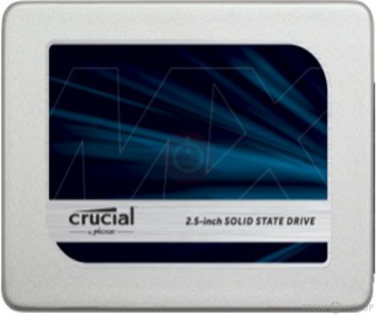
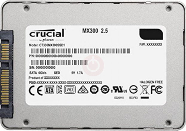
Crucial MX300 750 GB
750 GB
Capacity
88SS1074
Controller
TLC
Flash
SATA 6 Gbps
Interface
2.5"
Form Factor
Back
Package

PCB Front

PCB Back
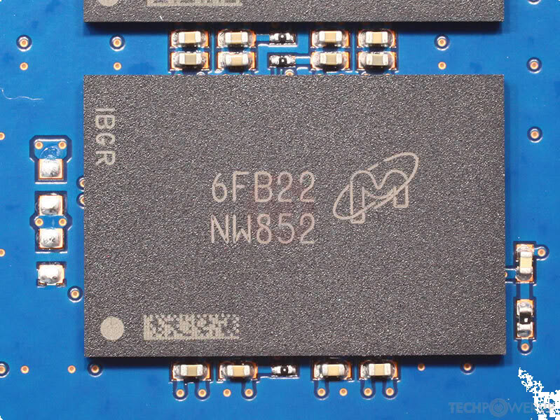
Flash
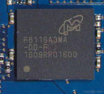
DRAM

Controller

NAND Die
The Crucial MX300 was a solid-state drive in the 2.5" form factor, launched in June 2016, that is no longer in production. It was available in capacities ranging from 275 GB to 2 TB. This page reports specifications for the 750 GB variant. With the rest of the system, the Crucial MX300 interfaces using a SATA 6 Gbps connection. The SSD controller is the 88SS1074 Dean from Marvell, a DRAM cache chip is available. Crucial has installed 32-layer TLC NAND flash on the MX300, the flash chips are made by Micron. To improve write speeds, a pseudo-SLC cache is used, so bursts of incoming writes are soaked up more quickly, once it is full, writes complete at 460 MB/s. The MX300 is rated for sequential read speeds of up to 530 MB/s and 510 MB/s write; random IOPS reach up to 92K for reads and 83K for writes.
At its launch, the SSD was priced at 180 USD. The warranty length is set to three years, which is above average, but shorter than the five years offered by many other vendors. Crucial guarantees an endurance rating of 220 TBW, a relatively low value compared to other SSDs.
At its launch, the SSD was priced at 180 USD. The warranty length is set to three years, which is above average, but shorter than the five years offered by many other vendors. Crucial guarantees an endurance rating of 220 TBW, a relatively low value compared to other SSDs.
Solid-State-Drive
| Capacity: | 750 GB |
|---|---|
| Variants: | 275 GB 525 GB 750 GB 1 TB 2 TB |
| Overprovisioning: | 69.5 GB / 10.0 % |
| Production: | End-of-life |
| Released: | Jun 2016 |
| Price at Launch: | 180 USD |
| Part Number: | CT750MX300SSD1 |
| Market: | Consumer |
Physical
| Form Factor: | 2.5" |
|---|---|
| Interface: | SATA 6 Gbps |
| Protocol: | AHCI |
| Power Draw: |
0.08 W (Idle) Unknown (Avg) 6.8 W (Max) |
Controller
| Manufacturer: | Marvell |
|---|---|
| Name: | 88SS1074 Dean |
| Architecture: | ARM 32-bit ARM9/ARMv5 |
| Core Count: | Dual-Core |
| Frequency: | 400 MHz |
| Foundry: | TSMC |
| Process: | 28 nm |
| Flash Channels: | 4 @ 400 MT/s |
| Chip Enables: | 8 |
| Controller Features: | DRAM (enabled) |
NAND Flash
| Manufacturer: | Micron |
|---|---|
| Name: | B0KB FortisFlash |
| Part Number: | NW852 (MT29F768G08EEHBBJ4-3R:B) |
| Type: | TLC |
| Technology: | 32-layer |
| Speed: | 50 MT/s .. 667 MT/s |
| Capacity: | 8 chips @ 768 Gbit |
| ONFI: | 4.0 |
| Topology: | Floating Gate |
| Die Size: | 168 mm² (2.3 Gbit/mm²) |
| Dies per Chip: | 2 dies @ 384 Gbit |
| Planes per Die: | 4 |
| Decks per Die: | 2 |
| Read Time (tR): | 92 µs |
| Program Time (tProg): | 2100 µs |
| Block Erase Time (tBERS): | 15 ms |
| Die Read Speed: | 695 MB/s |
| Die Write Speed: | 30 MB/s |
| Endurance: (up to) |
1500 P/E Cycles
(30000 in SLC Mode) |
| Page Size: | 16 KB |
| Block Size: | 1536 Pages |
| Plane Size: | 548 Blocks |
DRAM Cache
| Type: | LPDDR3-1333 CL11 |
|---|---|
| Name: | MICRON F8116A3MA-DD-F |
| Capacity: |
1024 MB
(1x 1024 MB) |
| Organization: | 8Gx16 |
Performance
| Sequential Read: | 530 MB/s |
|---|---|
| Sequential Write: | 510 MB/s |
| Random Read: | 92,000 IOPS |
| Random Write: | 83,000 IOPS |
| Endurance: | 220 TBW |
| Warranty: | 3 Years |
| MTBF: | 1.5 Million Hours |
| Drive Writes Per Day (DWPD): | 0.3 |
| SLC Write Cache: | Yes |
| Speed when Cache Exhausted: | approx. 460 MB/s |
Features
| TRIM: | Yes |
|---|---|
| SMART: | Yes |
| Power Loss Protection: | Yes |
| Encryption: |
|
| RGB Lighting: | No |
| PS5 Compatible: | No |
Reviews
Notes
Drive:MX300 uses small SMDs capacitors, which do not provide full protection from host power failures, but instead protect the data at rest. (backup circuitry that merely protects the existing data from corruption) NAND Die:tPROG with overhead: 1630 µs (Avg - 19.6 MB/s) |
Jun 1st, 2024 02:29 EDT
change timezone
Latest GPU Drivers
New Forum Posts
- what are these partitions and can they be removed? (2)
- DTS DCH Driver for Realtek HDA [DTS:X APO4 + DTS Interactive] (1919)
- RTX 3090 FE Caps Value??? (7)
- Where are the drives supposed to go? (37)
- What's your latest tech purchase? (20705)
- getting ready for dual 5090, Functional protype on dual 4090 (28)
- 3D/Game Design Workstation (2)
- Z890/X870 feature dreamlist (21)
- what HDD's work vertically ( too ) ? (24)
- No Post Debug Code 00 (20)
Popular Reviews
- ID-Cooling FX360 PRO Review - Shots Fired @ Arctic
- SilverStone KL07E Review
- NuPhy Air96 V2 Low Profile Wireless Mechanical Keyboard Review
- Senua’s Saga: Hellblade II: DLSS vs. FSR vs. XeSS Comparison Review
- Upcoming Hardware Launches 2024 (Updated May 2024)
- Montech Titan Gold 1000 W Review
- Waizowl OGM Cloud Review
- Elysian Acoustic Labs Pilgrim In-Ear Monitors Review
- Senua's Saga: Hellblade II Performance Benchmark Review
- Ghost of Tsushima Performance Benchmark Review - 35 GPUs Tested
Controversial News Posts
- AMD to Redesign Ray Tracing Hardware on RDNA 4 (227)
- NVIDIA to Only Launch the Flagship GeForce RTX 5090 in 2024, Rest of the Series in 2025 (154)
- AMD Hits Highest-Ever x86 CPU Market Share in Q1 2024 Across Desktop and Server (140)
- AMD RDNA 5 a "Clean Sheet" Graphics Architecture, RDNA 4 Merely Corrects a Bug Over RDNA 3 (139)
- NVIDIA RTX 5090 "Blackwell" Founders Edition to Implement the "RTX 4090 Ti" Cinderblock Design (115)
- Core Configurations of Intel Core Ultra 200 "Arrow Lake-S" Desktop Processors Surface (101)
- Biden Administration to Revive Trump-Era Tariffs on China-made GPUs and Motherboards (95)
- NVIDIA Testing GeForce RTX 50 Series "Blackwell" GPU Designs Ranging from 250 W to 600 W (84)