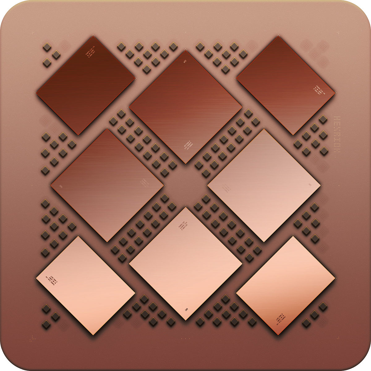
If you begin with 1 chiplet and n memory chips you can then move onto m chiplets and n * m memory modules.
While CUDA seems to have the programming API for this, I don't believe this is common in DirectX (11 or 12), OpenGL, or Vulcan code. Even then, I don't think that people typically use CUDA's memory management interface like this, because its only relevant on the extremely niche DGX-class of computers.
In contrast, CPU shared memory is almost completely transparent to the programmer. The OS could easily migrate your process to other chips (affinity settings notwithstanding). In fact, affinity settings were invented to prevent the OS from moving your process around.
I say "almost" completely transparent, because NUMA does exist if you really want to go there. But CPU programmers have gotten surprisingly far without ever worrying about NUMA details (unless you're the cream-of-the-crop optimizer. Its a very niche issue where most programmers simply trust the OS to do the right thing).
The software ecosystem that would support a multi-chipset architecture, with each chipset having an independent memory space, simply does not exist. Therein lies the problem: we either have to make a NUMA-like API where each chiplet has a NUMA-like memory space that the programmer has to manage.
OR, we build a crossbar, similar to AMD's Infinity Fabric (IFOP) which transparently copies data between chips... providing the programmer an illusion that all of the memory is in the same space.
50GBps is sufficient for AMD Infinity Fabric. For the same thing to happen on GPUs, NVidia has demonstrated that 300GBps is needed in their DGX-2 computers.
This isn't an easy problem, by any stretch of the imagination. I do imagine that it will be solved eventually, but I'm grossly interested in seeing how its done. I'm betting that NVidia will shrink their NVLink and NVSwitch system down and make it cheaper somehow.
A SIMD chiplet doesn't even make sense, SIMD needs centralized instruction dispatch and logic, modern GPUs aren't SIMD , meaning there isn't a 64*32bit wide vector register physically on the chip.
We've discussed this before Vya. Your understanding of GPU architecture is off.
AMD Vega (and all GCN processors) had the above memory diagram. The 256 VGPR registers were arranged in a 64 x 32-bit array called "SIMD 0". Vega's compute units are pretty complicated and there is also SIMD1, SIMD2, SIMD3 with independent instruction pointers.
The entire class of VGPRs operate in a SIMD fashion, as demonstrated by chapter 6.
So when you do an "v_add_F32 0, 1", this means all 64-values in VGPR#1 are added to all 64-values in VGPR#0, and then the result is stored into VGPR#0. Its a 64-wide SIMD operation. All "v" operations on Vega are 64-wide. RDNA changed this to a 32-wide operation instead. But the concept is similar.
I'm less familiar with NVidia's architecture, but I assume a similar effect happens with their PTX instructions.
With a GPU you are guaranteed that the CU in one chiplet does not need to communicate with a CU in another chiplet.
At a minimum, video games share textures. If Chiplet#1 has the texture for Gordon Freeman's face, but Chiplet#2 doesn't have it, how do you expect Chiplet#2 to render Gordon Freeman's face?
GPUs, as currently architected, have a unified memory space where all information is shared. Crossfire halved the effective memory, because to solve the above issue, they simply copied the texture to both GPUs. (IE: two 4GB GPUs will have a total of 4GBs of VRAM, because every piece of data will be replicated between the two systems). It was a dumb and crappy solution, but it worked for the purposes of Crossfire.
This is why inter-chip communications might happen. If you want Gordon Freeman's face to be rendered on Chiplet#1 and Chiplet#2 in parallel, you need a way to share that face-texture data between the two chips. This is the approach of NVidia's NVSwitch in the DGX-2 computer.
Alternatively, you could tell the programmer that Chiplet#2
cannot render Gordon Freeman's face because the data is unavailable. This would be a NUMA-like solution (the data exists only on chiplet#1). Its a harder programming model, but it can be done.
Or maybe a mix of the two approaches can happen. Or maybe a new system is invented in the next year or two. I dunno, but its a
problem. And I'm excited to wait and see what the GPU-architects will invent to solve the problem whenever chiplets arrive.


 .
.