- Joined
- Oct 9, 2007
- Messages
- 46,393 (7.67/day)
- Location
- Hyderabad, India
| System Name | RBMK-1000 |
|---|---|
| Processor | AMD Ryzen 7 5700G |
| Motherboard | ASUS ROG Strix B450-E Gaming |
| Cooling | DeepCool Gammax L240 V2 |
| Memory | 2x 8GB G.Skill Sniper X |
| Video Card(s) | Palit GeForce RTX 2080 SUPER GameRock |
| Storage | Western Digital Black NVMe 512GB |
| Display(s) | BenQ 1440p 60 Hz 27-inch |
| Case | Corsair Carbide 100R |
| Audio Device(s) | ASUS SupremeFX S1220A |
| Power Supply | Cooler Master MWE Gold 650W |
| Mouse | ASUS ROG Strix Impact |
| Keyboard | Gamdias Hermes E2 |
| Software | Windows 11 Pro |
Fujitsu Semiconductor Limited and SuVolta, Inc. today announced that they have successfully demonstrated ultra-low-voltage operation of SRAM (static random access memory) blocks down to 0.425V by integrating SuVolta's PowerShrink low-power CMOS platform into Fujitsu Semiconductor's low-power process technology. By reducing power consumption, these technologies will make possible the ultimate in "ecological" products in the near future. Technology details and results will be presented at the 2011 International Electron Devices Meeting (IEDM) being held in Washington DC, starting December 5th.
Controlling power consumption is the primary limiter of adding features to product types ranging from mobile electronics to tethered servers and networking equipment. The biggest contributor to power consumption is supply voltage. Previously, the power supply voltage of CMOS steadily reduced to approximately 1.0V at the 130nm technology node, but it has not reduced much further as technology has scaled to the 28nm node. To reduce the power supply voltage, one of the biggest obstacles is the minimum operating voltage of embedded SRAM blocks.

By combining SuVolta's Deeply Depleted Channel (DDC) transistor technology - a component of the PowerShrink platform - and Fujitsu Semiconductor's sophisticated process technology, the two companies have verified that a 576Kb SRAM can work well at approximately 0.4V by reducing CMOS transistor threshold voltage (VT) variation to half. This technology matches well with existing infrastructures including existing system-on-chip (SoC) design layouts, existing design schemes such as body bias control, and existing manufacturing tools.
Background
Following scaling law, the power supply voltage of CMOS has been reduced progressively down to approximately 1.0V at the 130nm technology node. However, power supply voltages have remained at around 1.0V even though process technologies have continued to scale from 130nm to 28nm. Since dynamic power is proportional to the square of supply voltage, power consumption has become a primary issue for CMOS technology. Scaling of supply voltage stopped at the 130nm node because of multiple sources of variation including random dopant fluctuation (RDF). RDF is a form of device and process variation resulting from fluctuations in the concentration of the implanted dopant or impurity atoms in the transistor channel. RDF results in variation in threshold voltage (VT) between different transistors on a chip.
Successful reduction of RDF has been reported using two exotic structures, ETSOI and Tri-Gate - a FinFET technology. However, both ETSOI and FinFET technologies are complex, making them difficult to match with existing design and manufacturing infrastructures.
SuVolta's DDC transistor
An implementation of SuVolta's DDC transistor on Fujitsu Semiconductor's low-power CMOS process is shown in figure 1. The cross sectional transmission electron micrograph (TEM) shows the transistor fabricated on a planar bulk silicon structure.
Figure 1. Cross-section of DDC transistor
Reduction of minimum operating voltage for SRAM
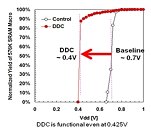
For most chips, lowering supply voltage is limited by the SRAM. Fujitsu Semiconductor and SuVolta have demonstrated an SRAM macro functional even at 0.425V, as seen in figure 2. Since SRAM is the most challenging circuit for supply voltage reduction, the verification implies that DDC could enable approximately 0.4V operation across a variety of CMOS-based circuits.
Figure 2 shows yield of 576k SRAM macro as a function of supply voltage. The yield is calculated by counting macros in which all bits have passed.
Summary and Future Plans
The process flow for DDC transistors has been successfully established. Fabricated DDC transistors demonstrate a 50 percent reduction of VT variation from the baseline flow, and deliver functional SRAMs even at 0.425V. These show the DDC transistors' capability to reduce supply voltage down to ~0.4V.
Fujitsu Semiconductor is going to advance the technology and aggressively respond to customers' requests for low-power consumption and/or low voltage operation in consumer products, mobile devices and other offerings.
View at TechPowerUp Main Site
Controlling power consumption is the primary limiter of adding features to product types ranging from mobile electronics to tethered servers and networking equipment. The biggest contributor to power consumption is supply voltage. Previously, the power supply voltage of CMOS steadily reduced to approximately 1.0V at the 130nm technology node, but it has not reduced much further as technology has scaled to the 28nm node. To reduce the power supply voltage, one of the biggest obstacles is the minimum operating voltage of embedded SRAM blocks.


By combining SuVolta's Deeply Depleted Channel (DDC) transistor technology - a component of the PowerShrink platform - and Fujitsu Semiconductor's sophisticated process technology, the two companies have verified that a 576Kb SRAM can work well at approximately 0.4V by reducing CMOS transistor threshold voltage (VT) variation to half. This technology matches well with existing infrastructures including existing system-on-chip (SoC) design layouts, existing design schemes such as body bias control, and existing manufacturing tools.
Background
Following scaling law, the power supply voltage of CMOS has been reduced progressively down to approximately 1.0V at the 130nm technology node. However, power supply voltages have remained at around 1.0V even though process technologies have continued to scale from 130nm to 28nm. Since dynamic power is proportional to the square of supply voltage, power consumption has become a primary issue for CMOS technology. Scaling of supply voltage stopped at the 130nm node because of multiple sources of variation including random dopant fluctuation (RDF). RDF is a form of device and process variation resulting from fluctuations in the concentration of the implanted dopant or impurity atoms in the transistor channel. RDF results in variation in threshold voltage (VT) between different transistors on a chip.
Successful reduction of RDF has been reported using two exotic structures, ETSOI and Tri-Gate - a FinFET technology. However, both ETSOI and FinFET technologies are complex, making them difficult to match with existing design and manufacturing infrastructures.
SuVolta's DDC transistor
An implementation of SuVolta's DDC transistor on Fujitsu Semiconductor's low-power CMOS process is shown in figure 1. The cross sectional transmission electron micrograph (TEM) shows the transistor fabricated on a planar bulk silicon structure.
Figure 1. Cross-section of DDC transistor
Reduction of minimum operating voltage for SRAM
For most chips, lowering supply voltage is limited by the SRAM. Fujitsu Semiconductor and SuVolta have demonstrated an SRAM macro functional even at 0.425V, as seen in figure 2. Since SRAM is the most challenging circuit for supply voltage reduction, the verification implies that DDC could enable approximately 0.4V operation across a variety of CMOS-based circuits.
Figure 2 shows yield of 576k SRAM macro as a function of supply voltage. The yield is calculated by counting macros in which all bits have passed.
Summary and Future Plans
The process flow for DDC transistors has been successfully established. Fabricated DDC transistors demonstrate a 50 percent reduction of VT variation from the baseline flow, and deliver functional SRAMs even at 0.425V. These show the DDC transistors' capability to reduce supply voltage down to ~0.4V.
Fujitsu Semiconductor is going to advance the technology and aggressively respond to customers' requests for low-power consumption and/or low voltage operation in consumer products, mobile devices and other offerings.
View at TechPowerUp Main Site
