• Welcome to TechPowerUp Forums, Guest! Please check out our forum guidelines for info related to our community.

Ever wondered whats inside your GPU?

T4C Fantasy

CPU & GPU DB Maintainer
Staff member
Joined
May 7, 2012
Messages
2,597 (0.54/day)
Location
Rhode Island
System Name Whaaaat Kiiiiiiid!
Processor Intel Core i9-14900K @ Default
Motherboard Gigabyte Z690 AORUS Elite AX DDR4
Cooling Corsair H150i AIO Cooler
Memory Corsair Dominator Platinum 128GB DDR4-3200
Video Card(s) EVGA GeForce RTX 3080 FTW3 ULTRA @ Default
Storage Samsung 970 PRO 512GB + Crucial MX500 2TB x3 + Crucial MX500 4TB + Samsung 980 PRO 1TB
Display(s) 27" LG 27MU67-B 4K, + 27" Acer Predator XB271HU 1440P
Case Thermaltake Core X9 Snow
Audio Device(s) Logitech G PRO X 2 Lightspeed
Power Supply SeaSonic Platinum 1050W Snow Silent
Mouse Logitech G903 Lightspeed
Keyboard Logitech G915 X Lightspeed
Software Windows 11 Pro
Benchmark Scores FFXV: 19329
Actual Size in 1080P, 96px DPI
GTX 1070 Founders Edition
(Actual Size)
001 GTX 1070 Founders Edition.jpg


GTX 1070 Founders Edition PCB
(Actual Size)
001a GTX 1070 PCB.jpg


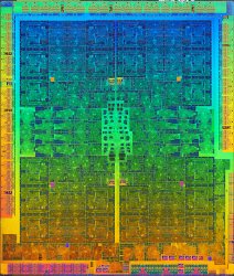
GP104-200-A1 Substrate & Die
(Actual Size)
03 GP104-200-A1.jpg


GP104-200-A1 Silicon Die (1920 Cuda Cores)
15 SM Clusters (Actual Size)
Marked GP104 Die
04 GP104-200-A1 Die.jpg


GP104-200-A1 SM Cluster (128 Cuda Cores)
(27x Magnification)
04a GP104-200-A1 Die SM.jpg


GP104-200-A1 (1 Cuda Core)
(27x Magnification)
04c GP104-200-A1 Die SM Single Core2.jpg


16nm FinFET Layout
05 FinFET layout.jpg


FinFET Cross sections
06 cross-section.jpg


FinFET transistor, this gpu has 7,200,000,000 of them
Samsung-14-LPE-FinFET-Trans-4.png


Attachment is largest size of the Silicon die i can put
Thanks! to Fouquin for providing the Silicon Die Shot
 

Attachments

  • GP104-200-A1 Die smaller3.jpg
    GP104-200-A1 Die smaller3.jpg
    1.5 MB · Views: 3,662
Last edited:
I always thought they ran on magic.

Seriously awesome stuff, thanks.
 
This stuff to fully understand exactly how everything is made, assembled, and works really does take some kind of engineering degree. Beyond me, all i know is what's faster in games.
 
I always thought they ran on magic.

Seriously awesome stuff, thanks.

I still can't comprehend how millions of transistors packed together into a chip can display beatiful games. I'm sure all this stuff is really just a coverup for pixie magic...
 
GPUs are actually made from dragon teeth.

You're welcome. :(
 
Are dragon teeth silicon?

That's kinda cool.
Ground up and heated/cooled many times to get the atoms happy and lined up. It's a very delicate process where the local bartender sometimes gets the batches a little wonky, hence the cards that don't OC worth a damn.
 
ok i got it, REAL size chip and die
03 GP104-200-A1.jpg


04 GP104-200-A1 Die.jpg


this is the size it would be if you seen it physically, the size it would be if you held xD so on etc.

actual size of a SM Cluster
04a GP104-200-A1 Die SM.jpg

this holds 128 Cuda Cores
 
Last edited:
Still seems to small for the package the GPU die resides on. I've seen plenty of bare GPU dies/packages from Nvidia, and AMD to know there consistently the same size for the package. The photo doesn't measure up to the actual size.
 
DID you see the size of them teeth on that rabbit?!!


06-cross-section-jpg.89740
 
Last edited:
Still seems to small for the package the GPU die resides on. I've seen plenty of bare GPU dies/packages from Nvidia, and AMD to know there consistently the same size for the package. The photo doesn't measure up to the actual size.
they are the same as package, i just layered it in photoshop
 
added actual size Card and PCB
 
Depends on what monitor you are using I guess. :)
It's rather small on my monitor.
i did it all on 4k monitor but this is all adjusted for 1080p

to put in perspective why i had to blow this pic up
GP104-200-A1 Die missing shit2.jpg
--->
04a GP104-200-A1 Die SM.jpg
--->
04c GP104-200-A1 Die SM Single Core2.jpg

|
v
04a GP104-200-A1 Die SM.jpg
 
Last edited:
20170702_054827.jpg

7870 XT 10.5inch PCB checking actual length comparison
 
Last edited:
No no gpu's are not made from dragon teefh or any other matrerial of magic or earfhly origin at all.

We all know the covered up alien chrash in roswell right. Gpu's aswell as cpu's is alien tech boys and girls.

Silicon come from the aliens as a gift to earfh and its people. The roswell cover up where because in return for silicon the goverment and military keeps the aliens a sercet so they cut leave earfh in peace.

So there you have it all :p

I think dragon teeth are way more plausible.
 
I took apart my gtx 750 ti to add a clean thing of thermal past o_O
 
I think dragon teeth are way more plausible.

Aliens are real. Havent you seen movies :p

We all know movies are all way the trufh.

Alright the real thing is silicon is a matrerial on earfh. No magic, alien or dragon about it.
 
GPUS, CPUS and other stuff are silicon based life form.

How much AI would a silicon chip need to be considered self aware and thus alive?
 
How much AI would a silicon chip need to be considered self aware and thus alive?

A good example would be when your GPU refuse to start a game "because it's already too hot in the damn room, and i'm not intending to run any hotter for your sake, human !"
 
now since GTX 1070 is partially disabled chip, can we see which part of the chip is disabled/cut off by laser ?
 
can we see which part of the chip is disabled/cut off by laser ?
The defects on die during lithography manufacturing process are in random locations. TSMC or Nvidia are not disabling a fixed location on die.
 
The die laser cuts were a thing of old, when they designed a chip with single or dual cores and it was easier to shine a laser on purpose built bridges if defects were found that cut power to certain areas of the die, or lowered the voltage to run at a maximum frequency limit, now its all done with software programming on EPROM or PROM memory on die, which is why certain motherboards could override the programmed model, core, and other configurations. Each chip gets tested either while still on the wafer or after cutting and they use either specially constructed traces through key parts of the die, or other tests to determine the quality of the die, and also why some people get chips that overclock amazing, and some get crap luck.
 
Back
Top