• Welcome to TechPowerUp Forums, Guest! Please check out our forum guidelines for info related to our community.

NVIDIA GeForce RTX 3090 "Ampere" Alleged PCB Picture Surfaces

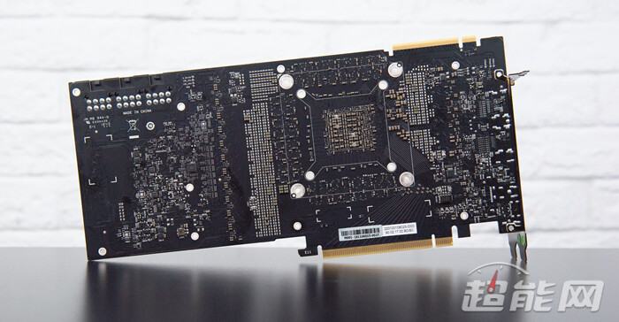
Memory in the back of the PCB? It's been a while since we've seen that on an Nvidia consumer board. 22GB of GDDR6 on a 352-bit bus?

My GTX 680 4GB had them on the back as well.
 

Attachments

  • pcb rtx 2080 ti vs rtx 3090 nvlink.jpg
    pcb rtx 2080 ti vs rtx 3090 nvlink.jpg
    147.8 KB · Views: 476
Can it handle 4k at 120fps with all settings maxed out?
 
It will be interesting to see how much power draw and heat matters this generation. I can sense a little walk back about how important they are...
 
Wow that card will cost a fortune.

And how do you cool that memory with its ~40 Watts thermal output without making the card a 4 slot monster because of a giant backplate...
 
3 x 8-pin .........

Quite an electric heater
Hi,
Might just mean it needs it's own source of power instead of sharing making the current more stable.
 
With 3X 8-PIN power connectors, this is a 500W+ card. Something wrong has happened with Ampere that they need to draw that much power to offer a generational leap over the 250-300W 2080 Ti. Yes, rumours are this is 40% faster than that card, but it draws about 40% more power. So the rumours of Nvidia going with the borked Samsung 8nm process instead of TSMC's superior 7nm+ appear true.

You're assuming maximum draw. It might have the ability to support that draw but might not have to.
 
There are leaks saying that 3090 (or whatever it is called) will target 350W peak power draw (PPD), BUT NVidia will allow user to remove power limiter, so that one can increase boost clock speeds past 2Ghz resulting in 400-500W PPD. It makes perfect sense if Ampere is on Samsung's 8nm node (comparable to 10nm TSMC's density). RDNA2 will boost at least to 2.23 GHz (confirmed by Sony's SP5 specs) on 7nm node so Ampere on 8nm will need A LOT of power draw to match it's frequency. I have no doubt Ampere's architecture would be much more power efficient than RDNA2's IF on 7nm, but Samsung's 8 nm is a big problem for Nvidia. We will likely see top tier Ampere GPUs migrating to 7 nm as soon as TSMC gives NVidia needed production capacities (probably in 2021 or 2022 when AMD Zen CPUs move to 5 nm).
 
Last edited:
May be NVidia figured out that to get rid of RT performance penalty, they need to throw another 150W at the problem. Or, it's a custom design. I am glad for a full 384-bit memory SKU again, unlike the compromised 320-bit and 352-bit ones we had been handed.
 
Last edited:
Well, you can also see that it has three 8-pin connectors. On a reference card ...

To me it's look like a pic of custom RTX2080ti. That nvlink finger is from Turing, not from Ampere. And that blurred image is just that, blurred.
 
3 x 8 pin, hmm, maybe it's the new 'macro transistor' technology intel is rumored to have developed :P
 
Obviously leak by Nvidia themselves. Real leak doesn't have blur boxes on them. Marketing BS.
 
It will be interesting to see how much power draw and heat matters this generation. I can sense a little walk back about how important they are...

Well hey, Vega 64 sold, offering GTX 1080 levels of performance despite being horrendously late and super juicy compared to the competition. I guess that's when undervolting became a hobby too.
 
Last edited:
nVidia hasn't had a *9* card since the dual-GPU GTX 690.
 
Back
Top