• Welcome to TechPowerUp Forums, Guest! Please check out our forum guidelines for info related to our community.

NVIDIA GK104 PCB Drawings, Unusual Power Connector Designs Surface

btarunr

Editor & Senior Moderator
Staff member
Joined
Oct 9, 2007
Messages
47,670 (7.43/day)
Location
Dublin, Ireland
System Name RBMK-1000
Processor AMD Ryzen 7 5700G
Motherboard Gigabyte B550 AORUS Elite V2
Cooling DeepCool Gammax L240 V2
Memory 2x 16GB DDR4-3200
Video Card(s) Galax RTX 4070 Ti EX
Storage Samsung 990 1TB
Display(s) BenQ 1440p 60 Hz 27-inch
Case Corsair Carbide 100R
Audio Device(s) ASUS SupremeFX S1220A
Power Supply Cooler Master MWE Gold 650W
Mouse ASUS ROG Strix Impact
Keyboard Gamdias Hermes E2
Software Windows 11 Pro
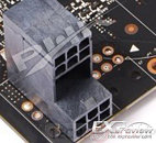
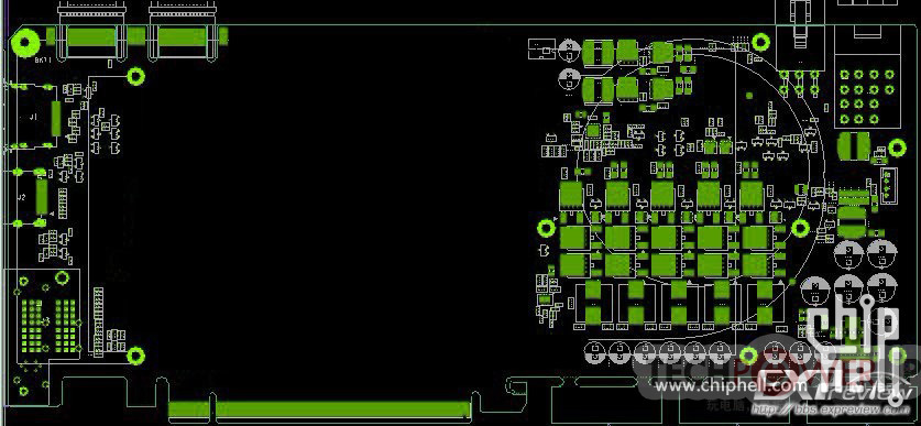
Here is the first x-ray drawing of NVIDIA's GeForce Kepler 104 (GK104) reference board, outlining the VRM area. The GPU and memory areas are blanked out for some very obvious reasons. Nevertheless, there's plenty of fascinating stuff going on in these pictures. To begin with, the picture confirms that the board will have 5 NVVDD phases, and up to three miscellaneous power domains. The PCB has provisions for two 6-pin and one 8-pin connector.

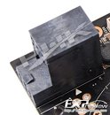
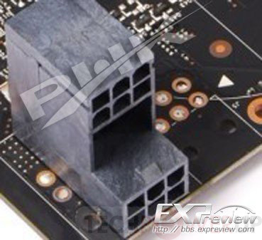
The funny part here is a strange new plug that has two 6-pin (or 8-pin+6-pin) stacked, while one of the two 6-pin connector leads are blanked. Some of our sources also report having seen a similar connector with 8-pin and 6-pin on samples of this card (refer to the last picture below). It's not just this, that makes the card incapable of single-slot operation, the DVI connectors over at the display IO also are stacked like on previous-generation AMD Radeon cards. Other connectors on the card are HDMI and DisplayPort. There are two SLI bridge connectors, giving it 3-way and 4-way SLI support.


View at TechPowerUp Main Site
 
The funny part here is a strange new plug that has two 6-pin (or 8-pin 6-pin) stacked

The monster shows its ugly head...
 
3-way sli support on a "4" series gpu....this is great.....

could you imagine what could have been with a tri-gtx 460/ 560 ti setup???
 
Aha! Now it makes all more sense, thanks Btarunr
 
So... with this new power conector you could put 4x8 pins on one card.
 
Stacked 8pin+6pin :shadedshu So how are we supposed to stack these into 4-way SLI on water again?
 
So it can do 8+6 pin side by side or 8+6 pin stacked, or are they talking about the top end cards needing 8+6+6 pin connectors?
 
I like how there is room on the PCB to add more power connectors. I have a feeling Kepler is going to be another power thirsty space heater for lack of a better phrase.
 
Title makes me think of Simon:laugh: Can't wait to see a working card cause a "drawing" does nothing for me.
 
Doc-Brown.jpg
 
I have a feeling Kepler is going to be another power thirsty space heater for lack of a better phrase.

good i will save on the heating bills then :laugh:
 
1.21 gigawatts indeed, punani.


I just hope that if it does use a large amount of power, it at least backs it up with proper performance. It's all we can ever ask for... and possibly a new surge protector, some new outlets, maybe even a larger breaker. All-in-all, still waiting to see what comes of it.
 
So AMD went for a minor overall increase in speed but with great efficency, and it looks like NVIDIA is going balls out performance if the PCB needs that much juice.
 
just throwing an idea out here, But those power connectors could be so you can link cards in the same circuit. So you can link cards 1 and 2 on a single rail, and cards 3 and 4 on your second sli rail.

The odd connection type could be Nvidias way of clearing up cables that they thought were unsightly.

The reason i say this is because of the green pcb layout. The 6/8 pin block stacks into the same connections on the pcb. If Nvidia were drawing that much power on these cards surely the connections would be independent, so as not to cross PSU rails.
 
something strange is going on
 
OMG... it will need nuclear reactor to power it in 4 way SLI :(
 
Yeah, if I'm seeing this correctly the PCB is setup for 6+6+8, though they are only using 6+6 at the moment(from the other thread). This leaves a lot of room for more powerful GPUs on this same PCB.
 
Another power hungry and inneficient card from nVidia.
 
Maybe they have decided to switch to a modular pcb design that can accommodate different setups mish-masing GPUsVRMs/RAMs etc...You know faster execution of new products and reduced Q&A/R&D at the cost of a few extra pennies per board.
 
Last edited:
Could this be the design for a possible dual GPU card that would need more power?
 
There is room for another 6 pin power connector
 
I dunno, the more i see this board the less i like it :o

Another power hungry and inneficient card from nVidia.

That is the main reason i have never went Nvidia in any of my build's. No one can say for certain just how efficient or inefficient this series will be but judging from Nvidia's history this will be more of the same :shadedshu
 
Who cares about efficiency on high end cards? Buy midrange if you want good perf/watt.
High end should bring loads of performance and IF possible efficiency, not necessarily anyway.
 
Back
Top