• Welcome to TechPowerUp Forums, Guest! Please check out our forum guidelines for info related to our community.

Haswell to Use 4th-Level On-Package Cache to Boost Graphics Performance

btarunr

Editor & Senior Moderator
Staff member
Joined
Oct 9, 2007
Messages
47,686 (7.42/day)
Location
Dublin, Ireland
System Name RBMK-1000
Processor AMD Ryzen 7 5700G
Motherboard Gigabyte B550 AORUS Elite V2
Cooling DeepCool Gammax L240 V2
Memory 2x 16GB DDR4-3200
Video Card(s) Galax RTX 4070 Ti EX
Storage Samsung 990 1TB
Display(s) BenQ 1440p 60 Hz 27-inch
Case Corsair Carbide 100R
Audio Device(s) ASUS SupremeFX S1220A
Power Supply Cooler Master MWE Gold 650W
Mouse ASUS ROG Strix Impact
Keyboard Gamdias Hermes E2
Software Windows 11 Pro
Intel is making serious efforts to boost CPU-integrated graphics performance using homegrown architectures, without having to borrow/license any technologies from the other two major players in the PC graphics business that have technological edges over Intel, and hence make high-performance discrete-GPUs (NVIDIA and AMD). Intel's architecture that succeeds Ivy Bridge, codenamed Haswell, will be at the receiving-end of a significant advancement in GPU performance.

We know from history, that Intel carves out variants of chips using a common silicon, by toggling the amount of L3 cache available, number of cores, and even number of iGPU shaders, apart from other natural handles such as clock speeds, voltages, and feature-set. With Haswell, the highest iGPU configuration will make use of a 4th-level cache (L4 cache), that sits on the package, while not being a part of the Haswell silicon. The Haswell silicon will instead be placed on a multi-chip module (MCM) along with a separate die that holds this L4 cache. The L4 cache will serve as a fast memory for the iGPU, while reducing or completely offloading the iGPU's dependency on the system memory as a frame-buffer (UMA).


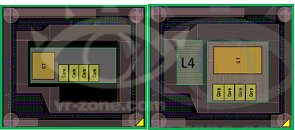
Such implementations aren't entirely new. IBM has used what's known as the eDRAM (embedded-DRAM), a separate silicon with fast memory and some low-level graphics logic, on some of its its game console processor ASICs. AMD, too, used a technology that's similar in principle, though not in implementation. Certain higher-end 7-series and 8-series graphics chipsets (such as AMD 780G, 790GX, and 890GX) feature what's known as DDR3-Sideport memory, which gives the Radeon IGP access to about 128 MB of fast DDR3 memory, which it can use standalone to offload system memory (UMA), or interleave with it (UMA+Sideport).

Could this be the what Intel is referring to as "Hotham 1.0"?

View at TechPowerUp Main Site
 
They could have solved this years ago by just simply...not using shared VRAM on everything. But, it is one thing to use this technique, its another to have the hardware to back it up. Not to mention drivers. I won't hold my breath for Intel to finally deliver on both fronts. If they can, great...more competition and better specs for hardware.
 
ahh, the tried and true intel method of solving cpu problems - if it sucks, slap on MOAR CACHE! :rockout:

jk :p
 
Anyspeculation as to what the size of this L4 cache is going to be ?

Is it actually going to be large enough to serve as dedicated video memory (= 256+ MB) ? IMHO such a solution would make the most sense, provided that there is enough room inside MCM for memory.
 
Might not need that much, remember the 360 used this technique. Think I remember it listed only 10MB of this ultrafast cache. Then you had 512MB shared with system and VRAM. Still, they used that with a high end level GPU (for the time period), not low end stuff. Till the tech is here to test, I wouldn't get too excited. AMD could easily counter this.
 
doubt it, a 256mb sram chip would be huge and cost a shitload. i say 32mb tops, even less.
 
Intel is known to be moving towards SoC design with Haswell and MCM could just mean that..
I guess 3D-stacking of modules could enable this.. it saves die area.. Ivy Bridge already has incorporated 3D stacking at the transistor level.. so 3D stacking at the die level(chip over chip) might just be the start with Haswell.. so it is not impossible for Intel to have a considerably large L4 cache (i am guessing at least 128MB) with 3D die stacking.. well, just guessing & i could be wrong as more information leaks/releases
 
so, i found an article about some mad ibm's processor with a 96mb L4 cache on a separate die. the die area was 487sq mm @ 45nm (1.5 billion transistors). so, if my maths aren't terribly wrong (sleep deprived and pretty stupid atm), they should be able to pack something like this in some 120-ish sq mm.

this is much more than i expected, i completely forgot about the 22nm process for haswell, this thing might actually end up with some 128mb of L4 cache :twitch:
 
... and Intel's Itanium(server) cpu already had a 'L4' cache back in 2004, codenamed Hondo.. it was 32MB.. and 'Poulson' codenamed 8-core expected in 2012 is expected to have the world's biggest L3 cache size — 54 MB. poulson chip is based on 32nm and die size is about 544 mm²

so, expecting a L4 cache >100MB with Haswell might not be too high..
 
I think that L4 could be a GDDR5 die. But I agree, such a big chunk of SRAM could drive up costs immensely.
 
Still only quad-core!

What this article also states is that the top end Haswell (within the mid-range) is still only going to be a quad core CPU!

By 2013/2014 that is going to be almost 8 years of mid-range CPUs having a maximum of 4 cores, come on people move things along!
 
What this article also states is that the top end Haswell (within the mid-range) is still only going to be a quad core CPU!
By 2013/2014 that is going to be almost 8 years of mid-range CPUs having a maximum of 4 cores, come on people move things along!

somewhat agree, but for single user desktops, the software that make use of all 4 cores is rare.. multi-thread/multi-core apps exist but not used by the average user.. even most games don't use more than 2 cores.. once the developers start leveraging the quad cores & threads then i guess we can demand for more cores..
 
I think that L4 could be a GDDR5 die. But I agree, such a big chunk of SRAM could drive up costs immensely.

you are probably right. In case of GPU it's better to add more cheaper memory
 
By 2013/2014 that is going to be almost 8 years of mid-range CPUs having a maximum of 4 cores, come on people move things along!
4 core is performance/price (manufacturing costs) sweet-spot and with HT it can take advantage of >4 thread support

if someone needs or think he/she needs more processing power then there are 6 and 8 core CPUs in the market... (and I'm not talking AMD here :shadedshu)
 
Yet another possibility is 32 MB of SRAM cache, which is big enough to be a frame-buffer, and fast enough to compensate for its size.
 
Yet another possibility is 32 MB of SRAM cache, which is big enough to be a frame-buffer, and fast enough to compensate for its size.

That will still highly rely on system memory though and only benefits you if you can swap pages in and out of cache before they're needed. I can't imagine a whole lot of speed benefits by doing this. The latency going from L3 to system memory isn't a huge leap and an L4 cache placement should be slower than L3 but faster than system memory... but the real question is how much bandwidth is there going to be and what will the latencies look like?

Looks like another reason why the BCLK on mainstream chips will have practically no wiggle room.
 
May teh force be with them, the 12 shaders that is :laugh:
 
So whilst Amd is trying to utilise system mem virtually for gfx in its apu.s and in the future on gfx cards intels finally goin old school tut. Tards
 
I think that L4 could be a GDDR5 die. But I agree, such a big chunk of SRAM could drive up costs immensely.

Note that GDDR5 isn't SRAM, it's DRAM, which means smaller die size and consequently cheaper production for a given capacity. Today's 1-2 GB video cards employ 8 chips, meaning one of those has capacity of 128-256 MB. Take away chip's package and the raw die has to be even smaller - perhaps just small enough to fit into an MCM, especially if produced on world's smallest lithography (where Intel has definite advantage over others).

With dedicated VRAM the GPU can scale up much more easily with the addition of more fucntional units as it is no longer constrained by the crappy memory bandwidth.

L4 cache approach on the other hand permits rather uniform performance with vastly larger memory pool (borrowed system RAM) but requires far more complicated control logic, even for EDRAM. And if they indeed went with SRAM that would mean more transistors still.

It will be interesting to see which way Intel went with Haswell, the cache way or VRAM way :)

Static ram is faster. This is another cache level, so I doubt there will be on-die dram. (That also adds temperature restrictions.)
 
I wonder why they don't do what AMD is doing, in that AMD has the IMC running at very fast speeds? Llano's IMC supports DDR3-1866, and I think Trinity's supports DDR3-2166. Now the AMD processor hardly benefits from that speed at all, but when using the integrated graphics, the memory bandwidth makes a huge difference in performance.

I'll admit it's annoying that laptop manufacturers like to put DDR3-1066/1333 in laptops where the processor supports much faster (so that'll have to be dealt with), but I could imagine an Intel Haswell Ultrabook with HD 5000 GPU and DDR3 2166 speeds (and 2166 modules to go with it) being quite useful.
 
Back
Top