• Welcome to TechPowerUp Forums, Guest! Please check out our forum guidelines for info related to our community.

AMD "Hawaii" Architecture Diagram Leaked

btarunr

Editor & Senior Moderator
Staff member
Joined
Oct 9, 2007
Messages
47,890 (7.38/day)
Location
Dublin, Ireland
System Name RBMK-1000
Processor AMD Ryzen 7 5700G
Motherboard Gigabyte B550 AORUS Elite V2
Cooling DeepCool Gammax L240 V2
Memory 2x 16GB DDR4-3200
Video Card(s) Galax RTX 4070 Ti EX
Storage Samsung 990 1TB
Display(s) BenQ 1440p 60 Hz 27-inch
Case Corsair Carbide 100R
Audio Device(s) ASUS SupremeFX S1220A
Power Supply Cooler Master MWE Gold 650W
Mouse ASUS ROG Strix Impact
Keyboard Gamdias Hermes E2
Software Windows 11 Pro
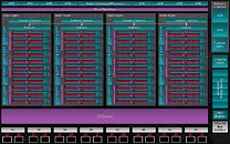
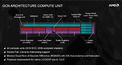
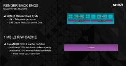
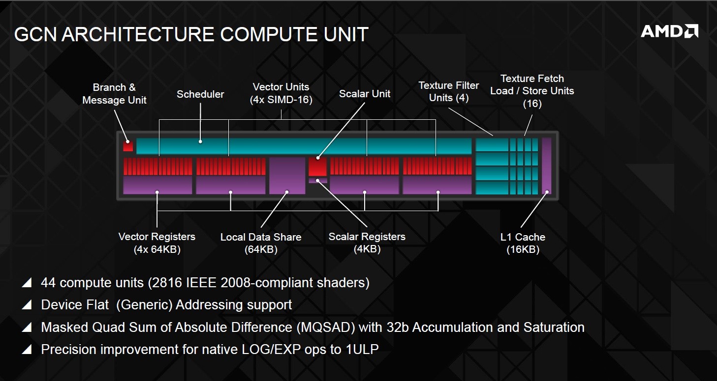
An alleged company slide detailing the architecture of AMD's upcoming "Hawaii" GPU was leaked to the web, revealing a monstrous combination of components. The GPU maintains the same component hierarchy as "Tahiti." The most distinguishing feature here is that whereas "Tahiti" features two shader engines, "Hawaii" features four. What it translates to, is double the geometry processing power, four independent geometry processors with a tessellation unit each, and double the number of ROPs, at 64. Each shader unit features 11 compute units (CU), the number-crunching machinery of the GPU. Each CU holds 4 TMUs (texture memory units), and 64 stream processors.

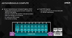
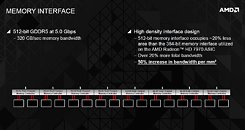
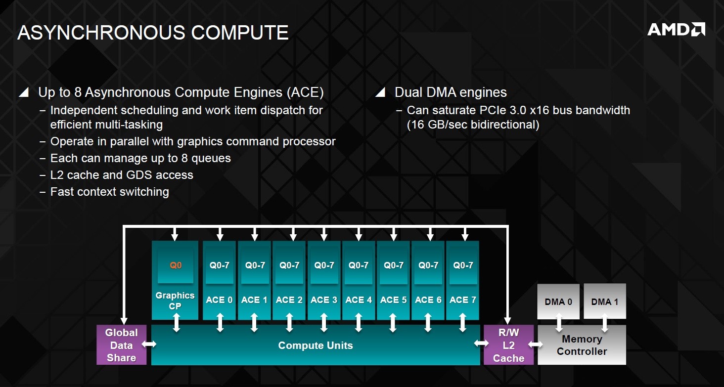
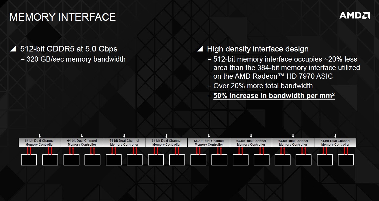
The four shader engines of "Hawaii" are tied to a unified command processing structure, a 1 megabyte L2 cache, a 512-bit wide GDDR5 memory interfaces, and the ancillaries, that include the PCI-Express 3.0 x16 bus interface, six display controllers (six TMDS links in all), CrossFireX XDMA, and multimedia accelerators that include UVD (accelerates high-def video), VCE (video codec engine, accelerates multimedia codecs), and the new TrueAudio hardware DSP.


View at TechPowerUp Main Site
 
That description just makes me want one of these even more :cry:
 
On paper this GPU seems be a computing beast. O_O
 
Last edited:
Interesting fact that this is still on 28nm :toast:

-=edited=-

The power density would have been too great on 22nm, it'd be extremely difficult to cool the GPU properly.

Don't confusing yourself with your uArch processor :slap:
it explain well you didn't have proper cooling for your own :troll: :nutkick:
 
Last edited:
The power density would have been too great on 22nm, it'd be extremely difficult to cool the GPU properly.
 
Yep, I want....

If somebody can tell me how a 512 bit memory interface uses less area than a 384 bit one that would be great.

I assume they're talking about the memory interface at the GPU end not the board.
 
A GPU with L2 cache...huh...thats something I didn't expect to see. Wonder if they did that based on their experience working with APUs.

If AMD wasn't rehashing some of the 7x00 series models for this gen then I'd almost think we may finally be coming out of the stagnation period that we've been in since Fermi launched. Not that it has been bad, we've had some great GPUs. But it is about time we moved on.
 
A GPU with L2 cache...huh...thats something I didn't expect to see. Wonder if they did that based on their experience working with APUs.

.

Its nothing new, I think its been around since ATI 5000 series.. Even 6?year old G80 aka 8800gtx had L1, L2 cache.


Its here mostly for compute and yeah its very small, obviously. :)
 
Last edited:
Really curious to see if 2 of these could take advantage of the extra lanes in a 4820k or a 4960x.
 
Yep, I want....

If somebody can tell me how a 512 bit memory interface uses less area than a 384 bit one that would be great.

I assume they're talking about the memory interface at the GPU end not the board.


It appears they optimized the memory interface since GCN 1.0 for GCN 1.1. Makes you wish they'd updated the 7970/R9 280X, 7950/R9 280, 7870/R9 270X, and 7850/R9 270 with GCN 1.1 just to see what improvements would have come from the optimization of diespace. If I recall correctly, the rumored improvements of Volcanic Islands (when it was a full GPU update instead of reheated leftovers with a new high end) were going to be "higher clockspeeds" and/or "smaller dies."

It kinda makes a bit more sense when given how optimized R9 290X seems to be.
 
If somebody can tell me how a 512 bit memory interface uses less area than a 384 bit one that would be great

the memory controller uses less silicon surface area _of the gpu_

the pcb with the memory controller signals will be much more complicated, crowded and expensive, more than a factor of two, when compared to 256 bit.
 
Freaking awesome!

512 bit bus width! That's freaking amazing. I wonder how much these will cost!
 
the memory controller uses less silicon surface area _of the gpu_

the pcb with the memory controller signals will be much more complicated, crowded and expensive, more than a factor of two, when compared to 256 bit.

very nice likeing the look of 8 Ace engines and 4 geometry/tess engines, anyone after a 7970:mad:
also 340Kb cache per Cu compute unit makes for a lot of on die cache x44
 
So....
2816 SP's at a clock speed of ??? (maybe 1050)
64 ROP's
176 TMU's
A Bus that is capable of 64 bytes (512 bits) in a single clock, and does 5 billion clocks in a second moving a substantial 320 Gigabytes in that second
Finally a pool of 4GB VRAM, wow :rockout:

Shaping up to be an amazing card, less TMU's then a GK110 based product though.
 
Shaping up to be an amazing card, less TMU's then a GK110 based product though.

But more ROPs, which means higher pixel fillrate, apparently +64 gpixel/s.,
I noticed Crysis, Crysis Warhead really likes higher pixel fillrates.


And from what saw higher TMU's matter only at higher resolution or multi monitor setup
 
If AMD can make a GPU = 7950 with no PCIE power pin and even less power consumption then I will take 2 :D
 
Back
Top