• Welcome to TechPowerUp Forums, Guest! Please check out our forum guidelines for info related to our community.
  • The forums have been upgraded with support for dark mode. By default it will follow the setting on your system/browser. You may override it by scrolling to the end of the page and clicking the gears icon.

Intel "Skylake" Die Layout Detailed

btarunr

Editor & Senior Moderator
Staff member
Joined
Oct 9, 2007
Messages
47,794 (7.40/day)
Location
Dublin, Ireland
System Name RBMK-1000
Processor AMD Ryzen 7 5700G
Motherboard Gigabyte B550 AORUS Elite V2
Cooling DeepCool Gammax L240 V2
Memory 2x 16GB DDR4-3200
Video Card(s) Galax RTX 4070 Ti EX
Storage Samsung 990 1TB
Display(s) BenQ 1440p 60 Hz 27-inch
Case Corsair Carbide 100R
Audio Device(s) ASUS SupremeFX S1220A
Power Supply Cooler Master MWE Gold 650W
Mouse ASUS ROG Strix Impact
Keyboard Gamdias Hermes E2
Software Windows 11 Pro
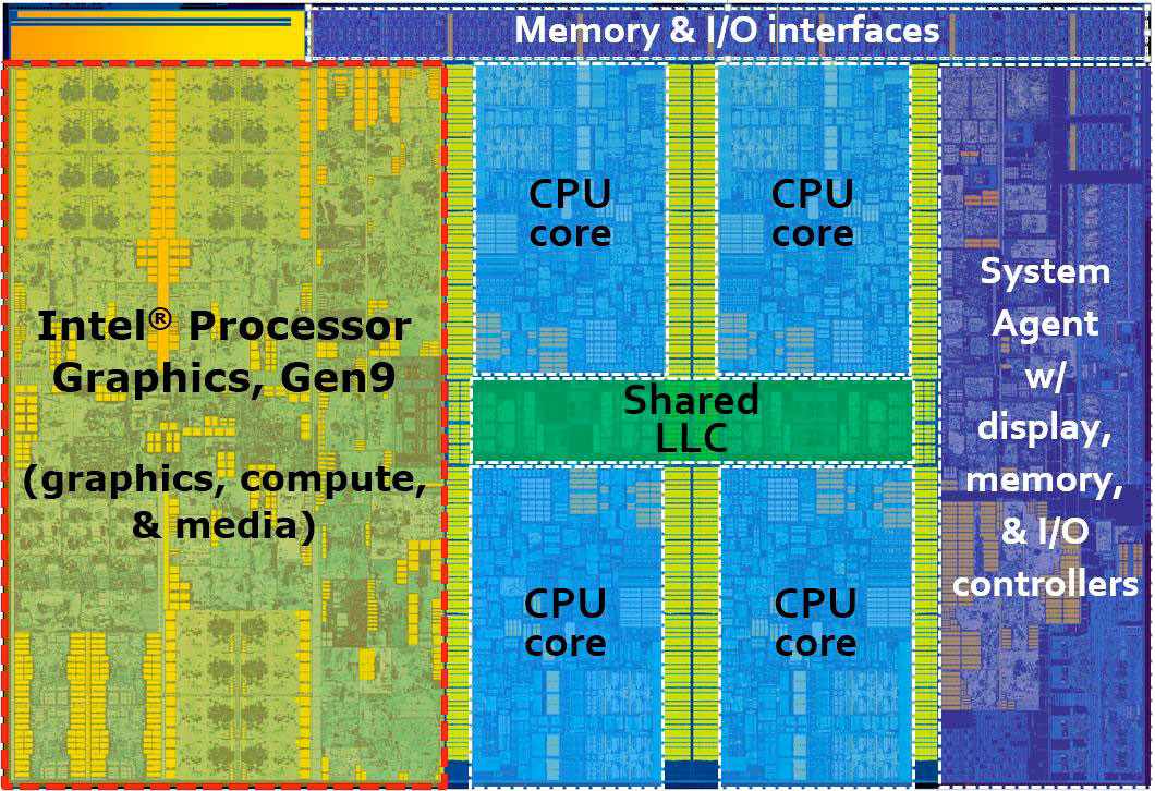
At the heart of the Core i7-6700K and Core i5-6600K quad-core processors, which made their debut at Gamescom earlier this month, is Intel's swanky new "Skylake-D" silicon, built on its new 14 nanometer silicon fab process. Intel released technical documents that give us a peek into the die layout of this chip. To begin with, the Skylake silicon is tiny, compared to its 22 nm predecessor, the Haswell-D (i7-4770K, i5-4670K, etc).

What also sets this chip apart from its predecessors, going all the way back to "Lynnfield" (and perhaps even "Nehalem,") is that it's a "square" die. The CPU component, made up of four cores based on the "Skylake" micro-architecture, is split into rows of two cores each, sitting across the chip's L3 cache. This is a departure from older layouts, in which a single file of four cores lined one side of the L3 cache. The integrated GPU, Intel's Gen9 iGPU core, takes up nearly as much die area as the CPU component. The uncore component (system agent, IMC, I/O, etc.) takes up the rest of the die. The integrated Gen9 iGPU features 24 execution units (EUs), spread across three EU-subslices of 8 EUs, each. This GPU supports DirectX 12 (feature level 12_1). We'll get you finer micro-architecture details very soon.


View at TechPowerUp Main Site
 
Wow, that's a lot of room dedicated just to the GPU. Bet those Xeons look great without that space taken up so they can cram cores!
 
.............In before the lame comments.......ITS ALL ABOUT THE GPU!!!!!!!!!!!!
 
I intend to disable the GPU via UEFI.
 

Look at the size of that GPU. It takes up more then 1/3 of the chip....I do not understand why a K class chip even has a freaking IGP. 90% of the people interested in K series run dedicated gpu. SO basically 35% of the cost of the chip is going towards an IGP that will never be used. I would much rather pay for 35% more cores. With the IGP gone it would be easy to fit in at least 2 more cores with out expanding the die.
 
That's unbelievable - 50% for graphics and 50% of the shared die area for the real stuff.

Of course, this sucks, and it sucks even worse when you know that Intel does nothing at least to try to develop software environment to unleash all those wasted transistors.
40% of the die - to be not used.
 
Last edited:
Is there any downside to having a disabled IGP there in terms of thermal/power usage?
 
Is there any downside to having a disabled IGP there in terms of thermal/power usage?
You just save power. That's it :)
 
You just save power. That's it :)

I meant is there a negative effect to have that dead-weight IGP there versus a chip that would completely cut out the IGP?
 
The IGP is this big not because Intel hopes you'll play Battlefront with it at 1080p. It's because Intel has to cope with the new wave of >1080p displays, such as 4K and 5K (particularly with high-res notebooks). This IGP has just enough juice to play 4K 60Hz video without stuttering. The API support is up-to-date just so you'll probably do DX12 asymmetric multi-GPU using discrete GPUs in the future, where your display is plugged into the IGP.
 
I meant is there a negative effect to have that dead-weight IGP there versus a chip that would completely cut out the IGP?
You can use quicksync to accelerate certain tasks that may not be coded in such a way to use your discrete card.
 
That's unbelievable - 50% for graphics and 50% of the shared die area for the real stuff.

Of course, this sucks, and it sucks even worse when you know that Intel does nothing at least to try to develop software environment to unleash all those wasted transistors.
40% of the die - to be not used.

I know!

I mean, I would know if I didn't know that Intel had provided developer guides since 2011:
https://software.intel.com/en-us/articles/intel-graphics-developers-guides

Or if I had missed when Intel put support behind OpenCL back in 2014:
http://streamcomputing.eu/blog/2014...opencl-as-the-heterogeneous-compute-solution/

Or didn't attend any of the numerous Intel-sponsored development events every year:
https://software.intel.com/en-us/
 
scumbag intel ....
 
I know!

I mean, I would know if I didn't know that Intel had provided developer guides since 2011:
https://software.intel.com/en-us/articles/intel-graphics-developers-guides

Or if I had missed when Intel put support behind OpenCL back in 2014:
http://streamcomputing.eu/blog/2014...opencl-as-the-heterogeneous-compute-solution/

Or didn't attend any of the numerous Intel-sponsored development events every year:
https://software.intel.com/en-us/

I see what you did there.
 
Waits for 8-core by intel
 

Attachments

  • skylala.jpg
    skylala.jpg
    84.7 KB · Views: 7,590
It's no secret Intel wants to go full SOC.

The only thing really missing is decent graphics. This is filling that gap. No, enthusiasts don't like it, but they also make up like 10% of the market if I'm being generous...
 
  • Like
Reactions: xvi
I'm sorry, Scumbag? For what exactly? Improving performance for users while lowering TDP?

I don't want a lower TDP with 10% performance increase. I want HUGE Performance gains and TDP doesn't matter at all. It's an i7 K chip. It should not be a power sipper and it also shouldn't have an IGP. However this is the first release at 14nm and hopefully the next release will ditch the IGP and go for more cores.
 
still not worth upgrading, intel made sandy bridge such a badass
 
still not worth upgrading, intel made sandy bridge such a badass
no sandies were soldered chips... this crappy new ones still use crappy paste...
 
You can always go for AMD... oops, I forgot they don't release a new chip for 3 years.

Joke apart that's exactly the problem: the Red team is not putting up a fight and Intel can do as they please.
Problem is, considering what AMD did with Fury I'm not hoping much for their next FX series (if there is one).
 
You just save power. That's it :)
Actually you don't.
Using a GPU while browsing, fapping, e.t.c. consumes much more power than having the iGPU enabled and turning on and off the dGPU for the heavy staff.
Also, your dGPU lives longer, unless you use nVidia and nVidia decides when to cripple your h/w.
 
I'm sorry, Scumbag? For what exactly? Improving performance for users while lowering TDP?

Thats the problem... intel does not improve the performance... not by much. Ever anymore.
 
I'm beating a dead horse here, but the intent of HEDT is to satisfy the exact conditions that most of you seem to expect from a top of the product stack mainstream i5/i7.

The complaints won't stop until Intel gets rid of the GPU, and they really won't stop because Intel is not going to take that GPU off. This die is going to power the other desktop i5s and i7s and those are parts intended for powering a 1080P monitor at work without the assistance of a dGPU. Not throwing money into the water for a pointless GPU-less Skylake design that basically gets them no $$$ at all is actually a pretty smart business plan, believe it or not.

Not a lot of praise where it's deserved, I'm afraid. I wouldn't be showering Intel with praise 24/7, but I didn't see any positive comments about the 5820K when it was released, only "only 28 PCIe lanes? What if I need the extra 12 to get maximum performance while getting off every day?" Tried to appease the enthusiasts with a 6-core HEDT part below $400, well, I guess that didn't work out very well, did it? The 5820K wasn't even a forced hand; it could very well have been a carbon copy of the 4820K, just on Haswell, as there are 4-core E5 V3s a-plenty to prove that.

Give people something better, and they'll find something better to complain about.
 
Last edited:
Thats the problem... intel does not improve the performance... not by much. Ever anymore.
thanks didnt saw the message!
you took my words...
point #2: intel knows pretty much the problem and differences about soldering and thermal paste on their CPU die's.....
but they still use that shitty paste... so?
 
Back
Top