- Joined
- Oct 9, 2007
- Messages
- 47,794 (7.40/day)
- Location
- Dublin, Ireland
| System Name | RBMK-1000 |
|---|---|
| Processor | AMD Ryzen 7 5700G |
| Motherboard | Gigabyte B550 AORUS Elite V2 |
| Cooling | DeepCool Gammax L240 V2 |
| Memory | 2x 16GB DDR4-3200 |
| Video Card(s) | Galax RTX 4070 Ti EX |
| Storage | Samsung 990 1TB |
| Display(s) | BenQ 1440p 60 Hz 27-inch |
| Case | Corsair Carbide 100R |
| Audio Device(s) | ASUS SupremeFX S1220A |
| Power Supply | Cooler Master MWE Gold 650W |
| Mouse | ASUS ROG Strix Impact |
| Keyboard | Gamdias Hermes E2 |
| Software | Windows 11 Pro |
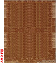
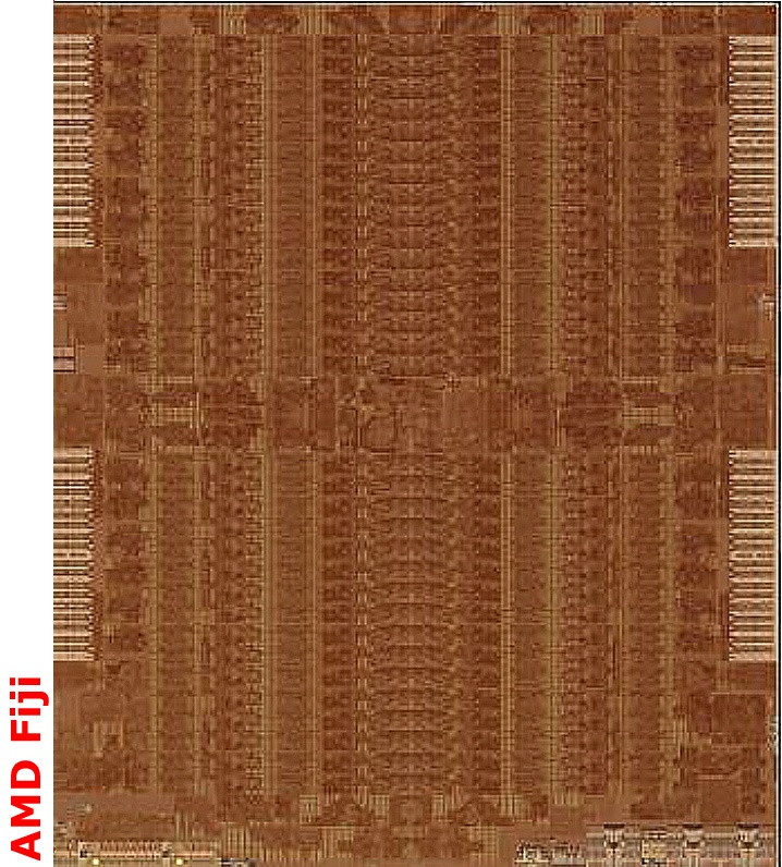
VLSI technical publication Chipworks posted the first clear die-shot of AMD's "Fiji" silicon, revealing intricate details of the most technically advanced GPU. What makes Fiji the most advanced graphics chip is its silicon interposer and stacked HBM chips making up a multi-chip module. It's the die in the center of all that, which went under Chipworks' microscope.
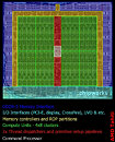
The die-shot reveals a component layout that's more or less an upscale of "Tonga." Some of the components, such as the front-end appear to be entirely identical to "Tahiti" or "Tonga." The shot reveals the 64 GCN compute units arranged in four rows, on either side of the central portion with the dispatch and primitive setup pipelines. The pad-area of the on-die memory controllers appear to be less than the large memory I/O pads that made up the 384-bit interface of "Tahiti." The first picture below is the die-shot of "Fiji," followed by a color-coded die-shot of "Tahiti."
View at TechPowerUp Main Site
The die-shot reveals a component layout that's more or less an upscale of "Tonga." Some of the components, such as the front-end appear to be entirely identical to "Tahiti" or "Tonga." The shot reveals the 64 GCN compute units arranged in four rows, on either side of the central portion with the dispatch and primitive setup pipelines. The pad-area of the on-die memory controllers appear to be less than the large memory I/O pads that made up the 384-bit interface of "Tahiti." The first picture below is the die-shot of "Fiji," followed by a color-coded die-shot of "Tahiti."

View at TechPowerUp Main Site


 True, but it's low-res photo. Of course for high-res you need to pay a lot.