• Welcome to TechPowerUp Forums, Guest! Please check out our forum guidelines for info related to our community.

Intel Core i7 "Broadwell-E" Lineup to Feature Four SKUs

btarunr

Editor & Senior Moderator
Staff member
Joined
Oct 9, 2007
Messages
47,670 (7.43/day)
Location
Dublin, Ireland
System Name RBMK-1000
Processor AMD Ryzen 7 5700G
Motherboard Gigabyte B550 AORUS Elite V2
Cooling DeepCool Gammax L240 V2
Memory 2x 16GB DDR4-3200
Video Card(s) Galax RTX 4070 Ti EX
Storage Samsung 990 1TB
Display(s) BenQ 1440p 60 Hz 27-inch
Case Corsair Carbide 100R
Audio Device(s) ASUS SupremeFX S1220A
Power Supply Cooler Master MWE Gold 650W
Mouse ASUS ROG Strix Impact
Keyboard Gamdias Hermes E2
Software Windows 11 Pro
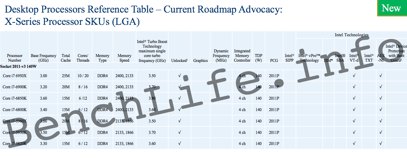
Intel is breaking away from its tradition of three Core i7 HEDT (high-end desktop) processors per generation, capturing price points of $400, $600, and $1000; with its upcoming Core i7 "Broadwell-E" HEDT lineup. According to leaked documents accessed by BenchLife.info, the company is readying four SKUs based on the 14 nm "Broadwell-E" silicon, these include the Core i7-6800K, the Core i7-6850K, the Core i7-6900K, and the Core i7-6950X.

The Core i7-6800K and i7-6850K are six-core chips, with HyperThreading enabling 12 logical CPUs, and 15 MB shared L3 cache. The i7-6800K is clocked at 3.40 GHz, with a 3.60 GHz Turbo Boost frequency. The i7-6850K is a notch above, with 3.60 GHz core, and 3.80 GHz Turbo Boost frequency. The slide doesn't mention if either of the two parts feature a limited PCIe root complex, like the one on the i7-5820K.


As we move up the lineup, there's the Core i7-6900K. This is an eight-core chip, with HyperThreading enabling 16 logical CPUs, and with 20 MB L3 cache at its disposal. Its core is clocked at 3.20 GHz, with a rather healthy 3.70 GHz Turbo Boost. At the very top of the lineup, is the Core i7-6950X. Intel's first consumer 10-core chip, with HyperThreading giving your OS a whopping 20 logical CPUs to deal with, this chip features 25 MB L3 cache, and is clocked at 3.00 GHz, with 3.50 GHz Turbo Boost.

All four chips in the lineup feature 140W TDP, unlocked base-clock multipliers, and will be compatible with existing socket LGA2011v3 motherboards with firmware updates. The low clock speeds on some of these chips right off the bat, could be Intel's way of not letting the rated TDP be higher than 140W. With the right cooling, the target consumers of these chips could overclock these chips.

Intel is planning to launch these Core i7 "Broadwell-E" chips in the second quarter of 2016.

View at TechPowerUp Main Site
 
Can't wait this is my next CPU Core i7-6900K or if I have extra cash I would go for the Core i7-6950X
 
The slide doesn't mention if either of the two parts feature a limited PCIe root complex, like the one on the i7-5820K

It mentioned "Up to 40 PCI-E 3.0 lanes"

One would assume "Up to" implies something is going to get gimped.
 
one in the eye for all those people that keep pushing skylake

they said skylake was the only way forward well......" INTEL SEEM TO DISAGREE"
 
Makes me wonder what the price point for the lower SKUs will be. Hoping this doesn't mean the X variant bumps to 1200 or higher (probably wishful thinking).
 
Sounds a little dubious to me that this supposed 6950X can only afford 2MB L3 per core. It's uncharacteristic of the HEDT lineage to have this, especially in such an expensive flagship. The 3930K and 4930K were only 2MB/core but they also weren't $1000 flagships.
 
one in the eye for all those people that keep pushing skylake

they said skylake was the only way forward well......" INTEL SEEM TO DISAGREE"
I'm waiting for Skylake-E, because everything I've seen about the architectural improvements, chipset and memory controller improvements have me wanting to wait.
 
lack of PCI-E 3.0 lanes in skylake is a problem ( only 16 for christ sake )
going foward that they need to solve
with more equipment uterlising PCIe ( add in cards ect ) there is going to be a bottleneck re available PCIx lanes

Hopefully thats something they need to sort out on the next release
 
Well, seems like I'll be waiting for 6900K.
 
14nm process and rated at 140W TDP. BUT the Broadwell-E 6 and 8 cores line up looks like a mirror image of the Haswell-E line up In terms of the base clock and L3 cache!

Looks like Broadwell-E is more of a "Haswell-E Refresh" ...
 
you had me until 140 watts, good grief why is the desktop counterpart so inefficient?

our 8 core 16 thread xeons are 55w the 18 core / 36 thread chips are 145w and they have 6 cores at 140w?

I don't get it
 
lack of PCI-E 3.0 lanes in skylake is a problem ( only 16 for christ sake )
going foward that they need to solve
with more equipment uterlising PCIe ( add in cards ect ) there is going to be a bottleneck re available PCIx lanes

Hopefully thats something they need to sort out on the next release

But Z170 offers another 20 PCIe 3.0 lanes. Compared to 5820K you actually get more PCIe 3.0 lanes to play with on 6700K.

In terms of actual configurations, 5820K has 16 + 8 PCIe 3.0 for graphics, 4 PCIe 3.0 for add-in cards and 8 PCIe 2.0 from X99 whereas 6700K has 8 + 8 PCIe 3.0 for graphics and 20 PCIe 3.0 from Z170 for everything else. If there are SLI/Xfire setup in your system, then 5820K is the winner here (although there is literally no performance difference between 16 + 8 and 8 + 8 for SLI/Xfire). For systems with a single graphics card, Z170 is actually more flexible. Also remember everything connected to the X99 PCH is limited by DMI 2.0.

Now Skylake-E will change the entire game with its upcoming X290 chipset (a guess for the name based on Intel naming convention).
 
you had me until 140 watts, good grief why is the desktop counterpart so inefficient?

our 8 core 16 thread xeons are 55w the 18 core / 36 thread chips are 145w and they have 6 cores at 140w?

I don't get it

It's because they use the better binned chips as Xeons.
 
you had me until 140 watts, good grief why is the desktop counterpart so inefficient?

our 8 core 16 thread xeons are 55w the 18 core / 36 thread chips are 145w and they have 6 cores at 140w?

I don't get it
Better binning, lower clock speeds, and lower voltages. Server/enterprise workloads can utilize 36 low speed threads a lot better than consumer workloads can.
 
It's because they use the better binned chips as Xeons.

Better binned might explain the difference between an 8 core at 105 and another at 140, but 55w 8 core vs 140w 6 core seems to indicate something far more than binning. I agree with Nelson Ng these seem like rebadges. Broadwell is no where near that inefficient.

now haswell on the other hand, that might make more sense. like my 4790k 4 cores at 88w vs 8 at 140 but with lower clocks that makes sense. The 6 core simply being the low bin of the bunch and the 10 core being the high bin.
 
I'm aware of that. It's about the PCIe configuration for the 16 lanes from 6700K CPU. Nothing to do with the 20 you get from Z170.
You get 4 2.0 from Z170 PCH, not 20. 20 lanes total is the 16 3.0 from the CPU and adding the 4x 2.0 from the PCH which is merely there for an M.2.

Edit: I should clarify, 4 usable. The Chipset provides but manufacturers designate the extra available lanes to other features of the board. On X99 you have Up to 40 lanes usable off the CPU itself while retaining the 8 2.0 lanes off the PCH. This in itself is more usable to the user if requiring a lot of expandability not offered on the board itself. The 5820k still offering more usable lanes even at a measly 28.
 
Last edited:
It mentioned "Up to 40 PCI-E 3.0 lanes"

One would assume "Up to" implies something is going to get gimped.
Like the 5820K I guess the 6800K would be the one that only has 28 PCI-e lanes compared to rest of the octa core bunch getting the whole 40 Lanes.
 
Sounds a little dubious to me that this supposed 6950X can only afford 2MB L3 per core. It's uncharacteristic of the HEDT lineage to have this, especially in such an expensive flagship. The 3930K and 4930K were only 2MB/core but they also weren't $1000 flagships.

You're correct, seems like it's a typo in the TPU article, as the 6950X has 25MB of cache.
Note that it's "total cache" not L3 as written in this article.
broadwell-e.jpg
 
Better binned might explain the difference between an 8 core at 105 and another at 140, but 55w 8 core vs 140w 6 core seems to indicate something far more than binning. I agree with Nelson Ng these seem like rebadges. Broadwell is no where near that inefficient.

now haswell on the other hand, that might make more sense. like my 4790k 4 cores at 88w vs 8 at 140 but with lower clocks that makes sense. The 6 core simply being the low bin of the bunch and the 10 core being the high bin.
What exactly is your point? These chips do clock a lot higher than these xeons. Apart from that they're more or less identical. You know that for a higher clock you probably need a higher voltage, right? The voltage to power consumption relation isn't exactly proportional, and as such you get another spec for your chip depending on your desired power/watt ratio. The most efficient chip isn't necessarily the fastest and more slower cores are not always the solution.
 
You get 4 2.0 from Z170 PCH, not 20. 20 lanes total is the 16 3.0 from the CPU and adding the 4x 2.0 from the PCH which is merely there for an M.2.

Edit: I should clarify, 4 usable. The Chipset provides but manufacturers designate the extra available lanes to other features of the board. On X99 you have Up to 40 lanes usable off the CPU itself while retaining the 8 2.0 lanes off the PCH. This in itself is more usable to the user if requiring a lot of expandability not offered on the board itself. The 5820k still offering more usable lanes even at a measly 28.

Actually, the Z170 chipset supports PCIe 3.0. It as a multiplexer of sorts, as you have four lanes from the CPU to the chipset, but the chipset has up to 20 available lanes, some of them are muxed with SATA, USB 3.0 and Gigabit Ethernet though.
PCH%20Allocation.png
 
You're correct, seems like it's a typo in the TPU article, as the 6950X has 25MB of cache.
Note that it's "total cache" not L3 as written in this article.
I bet this means the same. Total cache = L3.
On Intel Core architecture, the higher level caches include the lower level ones (L3 always has a copy of the contents of L2 and so on). So this probably means "usable cache", which is the same as L3.
 
What exactly is your point? These chips do clock a lot higher than these xeons. Apart from that they're more or less identical. You know that for a higher clock you probably need a higher voltage, right? The voltage to power consumption relation isn't exactly proportional, and as such you get another spec for your chip depending on your desired power/watt ratio. The most efficient chip isn't necessarily the fastest and more slower cores are not always the solution.
That 140w tdp on a 14nm 6 core in 2016 is ridiculous.

hell I'm all for performance but if semi trucks were getting 60 mpg on a new tech and were able to haul even more and you went to buy a consumer grade truck with the same tech and it got 10mpg wouldn't you be perturbed?
 
Actually, the Z170 chipset supports PCIe 3.0. It as a multiplexer of sorts, as you have four lanes from the CPU to the chipset, but the chipset has up to 20 available lanes, some of them are muxed with SATA, USB 3.0 and Gigabit Ethernet though.
Yes but the 4 lanes available are generally tied to an M.2 slot and are gimped to 2.0 4x, as I was saying how the manufacturer defines how these PCH lanes are allocated. For instance a Gen 3 Ultra slot will share lanes from the CPU side rather than PCH because the lanes in the PCH are tied to other features on the board. One example being http://www.newegg.com/Product/Produ...57501&cm_re=asrock_z97-_-13-157-501-_-Product where SLI (dual 8x) isn't an option, has no Ultra M.2, and the only M.2 slot on the board is Gen 2 coming off the PCH.
 
Back
Top