• Welcome to TechPowerUp Forums, Guest! Please check out our forum guidelines for info related to our community.

TSMC to Build New $15.7 Billion Fab in Taiwan, for 3 nm and 5 nm Chips

Raevenlord

News Editor
Joined
Aug 12, 2016
Messages
3,755 (1.18/day)
Location
Portugal
System Name The Ryzening
Processor AMD Ryzen 9 5900X
Motherboard MSI X570 MAG TOMAHAWK
Cooling Lian Li Galahad 360mm AIO
Memory 32 GB G.Skill Trident Z F4-3733 (4x 8 GB)
Video Card(s) Gigabyte RTX 3070 Ti
Storage Boot: Transcend MTE220S 2TB, Kintson A2000 1TB, Seagate Firewolf Pro 14 TB
Display(s) Acer Nitro VG270UP (1440p 144 Hz IPS)
Case Lian Li O11DX Dynamic White
Audio Device(s) iFi Audio Zen DAC
Power Supply Seasonic Focus+ 750 W
Mouse Cooler Master Masterkeys Lite L
Keyboard Cooler Master Masterkeys Lite L
Software Windows 10 x64
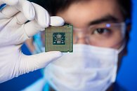
TSMC (Taiwan Semiconductor Manufacturing Co.), one of the foremost semiconductor producers in the world - which controls a leading 55% share of the global market - said on Wednesday it plans to build a new, $15.7 billion facility in Taiwan that would churn out 5 nm and 3 nm chips. If TSMC were to achieve these production nodes in a timely fashion (with "timely" meaning "before their competitors"), that would prove a huge boon for the company, as everyone - and especially deep-pocketed smartphone chip designers such as Apple and Qualcomm - is looking towards evolution in process nodes, which allows for improvements in power consumption, performance, size and cost of chips per wafer.

"We're asking the government to help us find a plot that is large enough (123 to 197 acres) and has convenient access so we can build an advanced chip plant to manufacture 5 nm and 3 nm chips," TSMC spokesperson Elizabeth Sun said. The spokesperson declined to provide details about the timing of the construction and production, though it's seemingly still a few years away (yet close enough for it to merit an official request). TSMC co-CEO Mark Liu had already mentioned that the company was working on 5 nm chips, and had assigned the task of developing 3 nm technology and conducting research on 2 nm technology to upwards of 300 engineers. Delays on EUV (Extreme Ultraviolet) lithography have slowed expected advancements in further miniaturization of the process nodes. It remains to be seen which technology TSMC is counting on towards aiding them in their goals for 5 nm, 3 nm and the mentioned 2 nm chip production, especially since at those sizes, we start leaving the usual realm of plane old physics, crossing the threshold towards their exotic cousins, quantum physics.


View at TechPowerUp Main Site
 
Last edited:
TSMC never beat anyone to any process node. What they need to do is follow closely. Beating the competition would be better, of course, but let's not get ahead of ourselves.
 
3nm and 5nm chips!? Is that even possible? At what point do they split the atom?

:toast:
 
It remains to be seen which technology TSMC is counting on towards aiding them in their goals for 5 nm, 3 nm and the mentioned 2 nm chip production, especially since at those sizes, we start leaving the usual realm of plane old physics, crossing the threshold towards their exotic cousins, quantum physics.
This is a little forced. Quantum size means sub-atomic sizes. Looooong way to go until there.
Just for the reference , the Silicon atom size is ~0.117nm, meaning you still have 9 atoms for each 1nm... and so on.
 
It's funny how second photo in news of TSMC shows Intel Pentium E2200 65nm CPU :)
 
This is a little forced. Quantum size means sub-atomic sizes. Looooong way to go until there.
Just for the reference , the Silicon atom size is ~0.117nm, meaning you still have 9 atoms for each 1nm... and so on.

gee, I wonder what are they going to do with all that quantum tunnelling
 
especially since at those sizes, we start leaving the usual realm of plane old physics, crossing the threshold towards their exotic cousins, quantum physics.

This is a false statement. Semiconductor electronics has always been based on quantum physics. Even a simple P-N junction diode (regardless of the manufacturing node) characteristics is derived from Fermi-Dirac distribution and Pauli exclusion principle.
 
I'm sure China is grateful for the new factory.
 
3nm and 5nm chips!? Is that even possible? At what point do they split the atom?

:toast:
I think a better question is what does that really mean.
 
Not the first ones tough.
 

Attachments

  • 1481443978645.jpg
    1481443978645.jpg
    402.9 KB · Views: 478
Well im holding off my playstation purchase until 5nm then. the pro slim ^2 version. And 3nm better be 2 years apart.
 
3nm and 5nm chips!? Is that even possible? At what point do they split the atom?

:toast:

Rule of thumb... for TSMC node sizes, double the number. (To equal intel's "real number) So 3nm and 5nm equal 6nm and 10nm... Intel is already working on that size of nodes. (Both TSMC and intel FAR IN THE FUTURE)

BTW, this rule of thumb only really applies to node sizes below TSMC 10nm...

I was wondering about the TSMC node sizes when apple stated that their processor was going to be made at node 10nm... thinking that TSMC beat Intel at the fab game, i googled it, happened upon an EE Times article "TSMC detail silicone road map" (would link it but the site eetimes site is "unavailable" )
And they mentioned that TSMC node sizes tend to be the minimum gate size, instead of the interconnect (metal) grid size ... (i believe intel states the interconnect size, thus the larger number)
 
Well im holding off my playstation purchase until 5nm then. the pro slim ^2 version. And 3nm better be 2 years apart.

Funny, yet they will ( most likely ) use TSMC's 7nm (14) process for ps5... although Sony did mention that the PS five will be a "clean slate"... not sure what that means, perhaps it means they don't want to be locked into a FAB (or processor?) and perhaps It might go to Intel or TSMC or whoever gives them an "offer they can't refuse" /lol
 
Funny, yet they will ( most likely ) use TSMC's 7nm (14) process for ps5... although Sony did mention that the PS five will be a "clean slate"... not sure what that means, perhaps it means they don't want to be locked into a FAB (or processor?) and perhaps It might go to Intel or TSMC or whoever gives them an "offer they can't refuse" /lol

If Sony goes Intel they drop backwards compatibility and devs would have to change their code again. Not to mention, Intel's Integrated GPUs suck. Why would they switch from AMD who has much better GPUs and significant experience integrating parts into consoles to Intel who has neither?
 
If Sony goes Intel they drop backwards compatibility and devs would have to change their code again. Not to mention, Intel's Integrated GPUs suck. Why would they switch from AMD who has much better GPUs and significant experience integrating parts into consoles to Intel who has neither?
What backwards compatibility? PS2 was MIPS, PS3 was POWER and now PS4 is x86_64. Going intel will actually preserve compatibility for a change.
 
Funny, yet they will ( most likely ) use TSMC's 7nm (14) process for ps5... although Sony did mention that the PS five will be a "clean slate"... not sure what that means, perhaps it means they don't want to be locked into a FAB (or processor?) and perhaps It might go to Intel or TSMC or whoever gives them an "offer they can't refuse" /lol
If Zen is half as a success as we expect it to be, you can bet Sony will not go with Intel. Getting all your essential parts from one place is god given. And by the time PS5 comes out HBM will be in full swing. Imagine what a evolved Zen apu with HBM can achieve.
 
Back
Top