• Welcome to TechPowerUp Forums, Guest! Please check out our forum guidelines for info related to our community.
  • The forums have been upgraded with support for dark mode. By default it will follow the setting on your system/browser. You may override it by scrolling to the end of the page and clicking the gears icon.

Intel Announces "Coffee Lake" + AMD "Vega" Multi-chip Modules

btarunr

Editor & Senior Moderator
Staff member
Joined
Oct 9, 2007
Messages
47,849 (7.39/day)
Location
Dublin, Ireland
System Name RBMK-1000
Processor AMD Ryzen 7 5700G
Motherboard Gigabyte B550 AORUS Elite V2
Cooling DeepCool Gammax L240 V2
Memory 2x 16GB DDR4-3200
Video Card(s) Galax RTX 4070 Ti EX
Storage Samsung 990 1TB
Display(s) BenQ 1440p 60 Hz 27-inch
Case Corsair Carbide 100R
Audio Device(s) ASUS SupremeFX S1220A
Power Supply Cooler Master MWE Gold 650W
Mouse ASUS ROG Strix Impact
Keyboard Gamdias Hermes E2
Software Windows 11 Pro
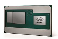
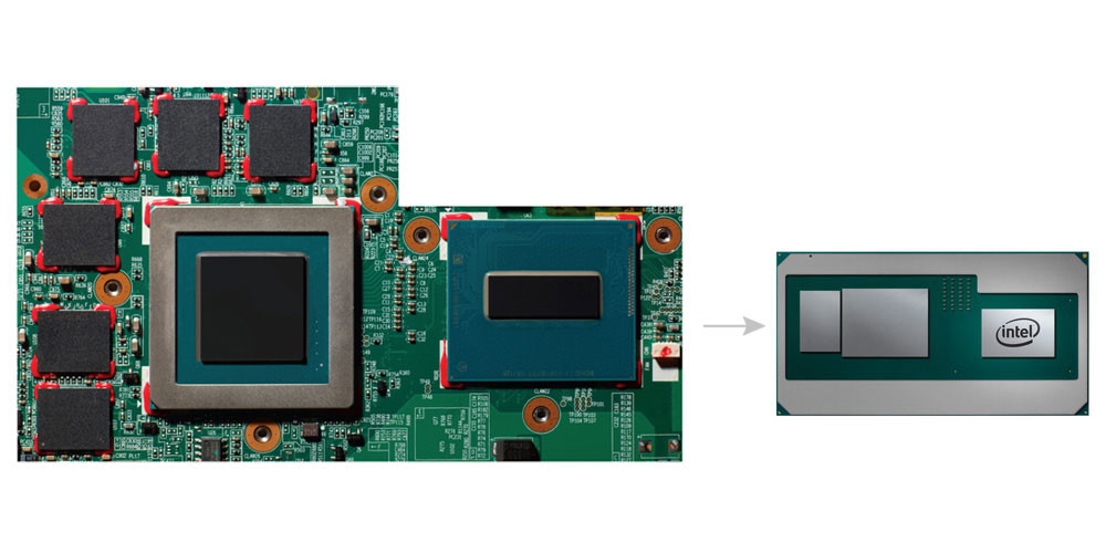
Rumors of the unthinkable silicon collaboration between Intel and AMD are true, as Intel announced its first multi-chip module (MCM), which combines a 14 nm Core "Coffee Lake-H" CPU die, with a specialized 14 nm GPU die by AMD, based on the "Vega" architecture. This GPU die has its own HBM2 memory stack over a 1024-bit wide memory bus. Unlike on the AMD "Vega 10" and "Fiji" MCMs, in which a silicon interposer is used to connect the GPU die to the memory stacks, Intel deployed the Embedded Multi-Die Interconnect Bridge (EMIB), a high-density substrate-level wiring. The CPU and GPU dies talk to each other over PCI-Express gen 3.0, wired through the package substrate.

This multi-chip module, with a tiny Z-height, significantly reduces the board footprint of the CPU + discrete graphics implementation, when compared to having separate CPU and GPU packages with the GPU having discrete GDDR memory chips, and enables a new breed of ultra portable notebooks that pack a solid graphics muscle. The MCM should enable devices as thin as 11 mm. The specifications of the CPU and dGPU dies remain under the wraps. The first devices with these MCMs will launch by Q1 2018.


A video presentation follows.


View at TechPowerUp Main Site
 
Last edited:
The CPU and GPU dies talk to each other over PCI-Express gen 3.0
This is where IF wins, less latency, more bandwidth & so much more possibilities.

A future AMD APU using HBM could will be a real monster.
 
RG0BS1U.gif


The rumors were indeed true.
 
23 Billion IOT devices by 2020 this means big investments in Data centers ect ect something nvda has been taking large market share from both Intel and AMD. This is only the start
 
Good to see this chip come to fruition.

I'm curious if Intel will at all be able to compete with the 15-30W TDP market but definitely be able to compete in the higher end market with this.

I think ryzen mobile really will kill it below 30 W but I don't see any product that will be that much better than intel's cpu when you add in the dedicated gpu.

Either way, good news for AMD.
 
I am sorry but this isn't April first
 
I'm curious if Intel will at all be able to compete with the 15-30W TDP market but definitely be able to compete in the higher end market with this.

I think ryzen mobile really will kill it below 30 W but I don't see any product that will be that much better than intel's cpu when you add in the dedicated gpu.

Either way, good news for AMD.
Ryzen Mobile targets a completely different market. Here we have a hi end CPU AND a hi end GPU, not a hi end CPU and a good enough GPU as it is with Ryzen.

I bet that OEMs explained to AMD that no matter how good Ryzen might be, it wouldn't get in many laptops for various reasons.

Intel needs a strong AMD as a shield against a huge Nvidia and AMD needs money and a bigger market share for it's GCN and FreeSync products.
 
This seems like a shot in the foot for AMD APUs
 
This is where IF wins, less latency, more bandwidth & so much more possibilities.

A future AMD APU using HBM could will be a real monster.
Less latency and more bandwidth than what?
 
Does this mean intel is retiring there own gpus?
 
Less latency and more bandwidth than what?
IF has theoretical max bandwidth of 512GBps, according to wiki, I assume it also has less latency wrt the solution that we're seeing today. Considering some of the results we've seen with Ryzen.
 
Cool, looking forward to when ASRock produces an STX board around this.
 
This seems like a shot in the foot for AMD APUs
There is ZERO impact on APUs... MCM = Multi-Chip Module, which is most definitely NOT an APU or even an iGPU... it's an Intel CPU and AMD GPU married together on a single substrate. This simple gets rid of GPU PCB, as well as the distance between the CPU and GPU electrically, which should allow for lower latency between the two separate pieces of silicon.

The news article even explains how this works, so I'm very perplexed at how you came to this conclusion...
 
Good for Intel. Not so bad for AMD. NVidia.. poor NVidia. :shadedshu:
 
I don't know much about MCM's but could they use something like this on PS5/XB2? Seems better than slow ass jaguar.
 
IF has theoretical max bandwidth of 512GBps, according to wiki, I assume it also has less latency wrt the solution that we're seeing today. Considering some of the results we've seen with Ryzen.
This thing is still connected over PCIe 3.0, so I'm not sure what exactly IF is supposed to improve here. Judging by your wording, you're not sure either.
 
IF has theoretical max bandwidth of 512GBps, according to wiki, I assume it also has less latency wrt the solution that we're seeing today. Considering some of the results we've seen with Ryzen.

This has the possibility of two distinct configurations as shown in the video if ONE HBM module is used (This is the reason why Vega runs HBM; R&D for laptops)
Well anyways, HBM 1 = 128 gb/sec, HBM 2 = 240 gb/sec ~

More than sufficient for laptops and HBM is power efficient and judging by ryzen mobile the vega chips can be very power efficient.

Ryzen mobile still stands to capture tons of sub 30w systems.
 
There is ZERO impact on APUs... MCM = Multi-Chip Module, which is most definitely NOT an APU or even an iGPU... it's an Intel CPU and AMD GPU married together on a single substrate. This simple gets rid of GPU PCB, as well as the distance between the CPU and GPU electrically, which should allow for lower latency between the two separate pieces of silicon.

The news article even explains how this works, so I'm very perplexed at how you came to this conclusion...
early nights late mornings :roll:
 
i really hope that amd will borrow that high density wiring from intel, and say goodbye to the interposer in discrete gpus too
 
It's on Intel's newroom page, so...
 
This is clearly a good fit for Apple, as they can easily squeeze this into a new ultra thin notebook and offer their customers decent graphics performance.

It is also a way for Intel to offer Apple a more appealing graphics solution until Apple decides to make their own "PC" CPU and dump Intel in the same way they dumped Imagination.

Finally it also explains why Apple doesn't have any notebook refreshes this year, as they were waiting for this.
 
This thing is still connected over PCIe 3.0, so I'm not sure what exactly IF is supposed to improve here. Judging by your wording, you're not sure either.
I understand that, I'm saying an AMD APU like this would only need IF to connect all the 3 on the same package. That should be higher bandwidth & likely less latency as well.
 
Back
Top