• Welcome to TechPowerUp Forums, Guest! Please check out our forum guidelines for info related to our community.

Intel NUC Based on Intel+Vega MCM Leaked

btarunr

Editor & Senior Moderator
Staff member
Joined
Oct 9, 2007
Messages
47,676 (7.43/day)
Location
Dublin, Ireland
System Name RBMK-1000
Processor AMD Ryzen 7 5700G
Motherboard Gigabyte B550 AORUS Elite V2
Cooling DeepCool Gammax L240 V2
Memory 2x 16GB DDR4-3200
Video Card(s) Galax RTX 4070 Ti EX
Storage Samsung 990 1TB
Display(s) BenQ 1440p 60 Hz 27-inch
Case Corsair Carbide 100R
Audio Device(s) ASUS SupremeFX S1220A
Power Supply Cooler Master MWE Gold 650W
Mouse ASUS ROG Strix Impact
Keyboard Gamdias Hermes E2
Software Windows 11 Pro
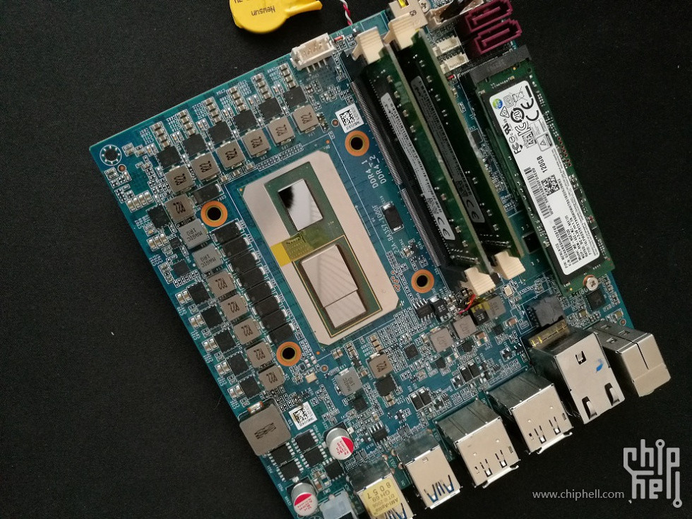
The first product based on Intel's ambitious "Kaby Lake-G" multi-chip module, which combines a quad-core "Kaby Lake-H" die with a graphics die based on AMD "Vega" architecture, will be a NUC (next unit of computing), and likely the spiritual successor to Intel's "Skull Canyon" NUC. The first picture of the motherboard of this NUC was leaked to the web, revealing a board that's only slightly smaller than the mini-ITX form-factor.

The board draws power from an external power brick, and appears to feature two distinct VRM areas for the CPU and GPU components of the "Kaby Lake-G" MCM SoC. The board feature two DDR4 SO-DIMM slots which are populated with dual-channel memory, and an M.2 NVMe slot, holding an SSD. There are two additional SATA 6 Gb/s ports, besides a plethora of other connectivity options.


View at TechPowerUp Main Site
 
That looks awesome! I'd put one in my car.
 
That looks too big to be a NUC, Mini-STX maybe?
Keep in mind that the NUC boards of today at least have the CPU on the bottom of the PCB as well, which clearly isn't the case here.
 
Last edited:
That looks too big to be a NUC, Mini-STX maybe?

"Skull Canyon" had a rather big PCB too, and yet was branded NUC. But you're right, this thing has too big Z-height. It looks more like a Zotac ZBOX.

12-nuc-open.jpg
 
Basically nextgen Skulltrail NUC, that would certainly be useful as console replacement.
 
"Skull Canyon" had a rather big PCB too, and yet was branded NUC. But you're right, this thing has too big Z-height. It looks more like a Zotac ZBOX.

Yeah, that seems very likely, as both the colour scheme and the model name appears similar to what Zotac uses. One of their other products start with 23A- as well.
 
Looks legit. There's even a piece of kapton tape covering caps on the module. The new Magnus?

How much would a NUC like that cost?
Probably the same, if not more, than the Skull Canyon NUC: starting at $600 and up.
 
Last edited:
Am I the only one noticing the seemingly 14-phase VRM around tue processing unit?
 
From my fanboy opinion this looks like a pretty awesome mini setup !!
jeezus, shrinking sizes with power like this oh my ......
 
Am I the only one noticing the seemingly 14-phase VRM around tue processing unit?
Not surprising at all.
You have to consider that you have a discrete GPU w/ HBM2 and a CPU on the same die.
It's not as much about power delivery, but supplying different voltages to various components.
Just by looking at it you can see your usual grouping:
* 4+1 for GPU
* 2 for HBM
* 1 for something
* 2 SoC (cause the entire hub is integrated into CPU die)
* 4 CPU vCore

The other coils that are scattered around the MoBo are from the power supply circuitry (12V, 5V, 5VSB, 3.3V, 1.8V etc).
The only thing that it shows, is that there is a full desktop CPU/GPU combo on that module, and not some underwhelming 15W PoS mobile CPU w/ lowest-of-the-low-end vega.
 
This chip is huge it's almost as big as a mini board with decent CPU+dGPU+Ram
 
Well, this definitely corroborates Intel's claims of board space savings. I'd like to see anyone implement a quad core CPU + dGPU of any kind in that kind of area. The great thing is that this - with some relatively minor additions for battery connectivity/charging and such, horizontal memory slots, and the I/O spread out/moved to a daughterboard - could slot into a 13" laptop with relative ease. It wouldn't be super thin, but the cooling required for a >65W CPU+GPU combo would make that impossible anyhow. Still, 1.6-2cm with dual fans and heatsinks, and a good complement of heatpipes, and you'd have a killer laptop for sure. I'd buy one (if it was from a decent brand and had a flippable, pen-enabled screen, that is).

Then again, I'd be perfectly happy with a well-cooled 25W Raven Ridge - sorry, Ryzen Mobile with Vega Graphics - in the same form factor.

You listening, OEMs?
 
This chip is huge it's almost as big as a mini board with decent CPU+dGPU+Ram
Are you joking? Those are SODIMM RAM slots next to it. Sure, it's bigger than a regular mobile CPU, but not massively. Eyeball "measurements" based on DDR4 SODIMMs being 69.6mm long places it at ... something like 55x30-60x35mm. That's tiny, way smaller than a credit card.
 
GPU+HBM2 sits on its own PCB on top of the CPU PCB ot top of the motherboard PCB, still long way from ideal solution but if they insist on it. Not a real integrated video. That is why they can't move all the chips close together but rather go for this strange GPU location, which either way is still on a separate PCB. Now if they produced this GPU on 10nm intel process it would be a different story, but no, they just bought a descrete GPU and soldered it next to the CPU and call it a day.
 
Last edited:
A good nuc costs 700$. How much for this? 1400$?
 
GPU+HBM2 sits on its own PCB on top of the CPU PCB ot top of the motherboard PCB, still long way from ideal solution but if they insist on it. Not a real integrated video. That is why they can't move all the chips close together but rather go for this strange GPU location, which either way is still on a separate PCB. Now if they produced this GPU on 10nm intel process it would be a different story, but no, they just bought a descrete GPU and soldered it next to the CPU and call it a day.
Are you proposing they stop putting CPU dice on substrates, and solder them directly to the motherboard? That would increase motherboard complexity and production costs enormously, if it were possible at all.

Also: no, the GPU and HBM2 are not on their own PCB on top of the substrate - the substrate links all three, with an EMIB interconnect embedded into the substrate for data transfer between the GPU and HBM. Look at the renders from the original announcement: https://www.anandtech.com/show/1200...with-amd-radeon-graphics-with-hbm2-using-emib

Sure, these are renders, but there's no reason for them to not be relatively visually accurate, and there is no visible distinction between the CPU and GPU substrates. If i were to guess, the gold outline seen here is some sort of guide for automated chip mounting systems, if not for cooler orientation or some other reason. Another argument from Intel for this is lower Z-height, which a second substrate would ruin. Not to mention that cooler mounting and manufacture would be greatly complicated with several different heights for the chips (just look at the issues surrounding the slight variations between different AMD Vega parts, which have far lower variance than a separate substrate would infer).

And nobody has called this "integrated video". Intel specifically calls it a "discrete graphics chip".

Lastly: the reason for the distance between the CPU and GPU is in all likelihood cooling: if this is a 30-50W+ GPU, sticking it right next to the 30-45W CPU would be downright silly. It's easier to fit more heatpipes over a more spread-out area, after all, and needlessly creating difficult-to-cool hotspots is just silly.
 
A good nuc costs 700$. How much for this? 1400$?
The Skull Canyon NUC barebones is $599. RAM and SSD costs are the same regardless of the base NUC (outside of the sheer silliness of sticking a 960 Pro in an i3 NUC or similar). If I were to guess, this would probably add another $100-200 to that. But of course, Intel does love to price premium parts into oblivion.
 
GPU+HBM2 sits on its own PCB on top of the CPU PCB ot top of the motherboard PCB, still long way from ideal solution but if they insist on it. Not a real integrated video. That is why they can't move all the chips close together but rather go for this strange GPU location, which either way is still on a separate PCB. Now if they produced this GPU on 10nm intel process it would be a different story, but no, they just bought a descrete GPU and soldered it next to the CPU and call it a day.
Intel "super glued" a discrete GPU and call it a day...
 
Are you proposing they stop putting CPU dice on substrates, and solder them directly to the motherboard? That would increase motherboard complexity and production costs enormously, if it were possible at all.

Also: no, the GPU and HBM2 are not on their own PCB on top of the substrate - the substrate links all three, with an EMIB interconnect embedded into the substrate for data transfer between the GPU and HBM. Look at the renders from the original announcement: https://www.anandtech.com/show/1200...with-amd-radeon-graphics-with-hbm2-using-emib

Sure, these are renders, but there's no reason for them to not be relatively visually accurate, and there is no visible distinction between the CPU and GPU substrates. If i were to guess, the gold outline seen here is some sort of guide for automated chip mounting systems, if not for cooler orientation or some other reason. Another argument from Intel for this is lower Z-height, which a second substrate would ruin. Not to mention that cooler mounting and manufacture would be greatly complicated with several different heights for the chips (just look at the issues surrounding the slight variations between different AMD Vega parts, which have far lower variance than a separate substrate would infer).

And nobody has called this "integrated video". Intel specifically calls it a "discrete graphics chip".

Lastly: the reason for the distance between the CPU and GPU is in all likelihood cooling: if this is a 30-50W+ GPU, sticking it right next to the 30-45W CPU would be downright silly. It's easier to fit more heatpipes over a more spread-out area, after all, and needlessly creating difficult-to-cool hotspots is just silly.


If you are talking about socket VS soldered it reduces motherboard complexity to be soldered, as it is now you have to have a whole pin structure that is spring loaded and solders onto-into the motherboard, and you have to use a retainer that will prevent the board from flexing deferentially to the socket and pin mechanism, and also can provide clamping and holding pressure for the CPU to the socket interface. There is literally nothing the socket provides beyond ease of assembly, end user choice and a reduced liability on the part of Intel when a socket dies or fails. Fewer components reduces rate of failure in general, and fewer components are easier to engineer than how more components will interact together.

For these to be soldered directly to the motherboard is equal to or less complex than adding another layer to the PCB and more vias.
Not what I was talking about whatsoever. I was responding to a post saying this seemingly had PCBs stacked up the bejeezus (which it doesn't), to which I pointed that out and asked whether the poster meant that the dice should be soldered straight to the motherboard, sans substrate - which would be the "logical" (though practically impossible) solution if CPU substrates are such an issue (which they aren't). I never mentioned a socket, as mobile chips haven't been socketed for years, and Intel sure isn't going to custom design an oddball rectangular socket for a two-SKU product series.

Then again, soldering a socket to the motherboard isn't really more complex than soldering on a BGA package, as the socket itself is usually just that - a BGA package, only one consisting of a grid of pins with solder ball "feet" in a plastic frame, rather than a PCB substrate. The retention bracket on LGA sockets are probably a bit of a hassle, though. Also, BGA grids can be far more dense than any grid of pins (whether LGA or PGA), at least at the same cost/complexity.
 
Not surprising at all.
You have to consider that you have a discrete GPU w/ HBM2 and a CPU on the same die.
It's not as much about power delivery, but supplying different voltages to various components.
Just by looking at it you can see your usual grouping:
* 4+1 for GPU
* 2 for HBM
* 1 for something
* 2 SoC (cause the entire hub is integrated into CPU die)
* 4 CPU vCore

The other coils that are scattered around the MoBo are from the power supply circuitry (12V, 5V, 5VSB, 3.3V, 1.8V etc).
The only thing that it shows, is that there is a full desktop CPU/GPU combo on that module, and not some underwhelming 15W PoS mobile CPU w/ lowest-of-the-low-end vega.
All of that is going to need cooling. I don't see this and the cooling solution fitting into a "NUC" form factor case. It'll likely be some variation of mini-ITX.
 
Back
Top