Raevenlord
News Editor
- Joined
- Aug 12, 2016
- Messages
- 3,755 (1.15/day)
- Location
- Portugal
| System Name | The Ryzening |
|---|---|
| Processor | AMD Ryzen 9 5900X |
| Motherboard | MSI X570 MAG TOMAHAWK |
| Cooling | Lian Li Galahad 360mm AIO |
| Memory | 32 GB G.Skill Trident Z F4-3733 (4x 8 GB) |
| Video Card(s) | Gigabyte RTX 3070 Ti |
| Storage | Boot: Transcend MTE220S 2TB, Kintson A2000 1TB, Seagate Firewolf Pro 14 TB |
| Display(s) | Acer Nitro VG270UP (1440p 144 Hz IPS) |
| Case | Lian Li O11DX Dynamic White |
| Audio Device(s) | iFi Audio Zen DAC |
| Power Supply | Seasonic Focus+ 750 W |
| Mouse | Cooler Master Masterkeys Lite L |
| Keyboard | Cooler Master Masterkeys Lite L |
| Software | Windows 10 x64 |
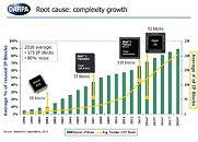
EDA (Electronic Design Automation) is a quintessential part of modern silicon processor design - of any kind. Be it GPUs, CPUs, or SOCs, you can bet an electronic design tool has been applied somewhere in the process. These tools serve their function in various steps of silicon design, be it allowing for automated placement of components, signal routing, power optimization, and analyzing said designs with performance and bottleneck projections. It was rumored that Bulldozer was such a flawed architecture due to the overuse (and misuse) of EDA tools in its design; but mostly, usage of these tools is done in conjunction with engineers' hand-crafted, manually laid-out circuits.
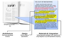
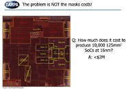
In an effort to accelerate development and reduce cost of chip design (now approaching $500 million for a bleeding-edge SoC), two programs, IDEA (Intelligent Design of Electronic Assets) and POSH (Posh Open Source Hardware), involving 15 companies and more than 200 researchers, will receive $100 million in funding over the next five years. The IDEA is to create the equivalent of a silicon compiler, aimed at significantly lowering the barriers to design chips. POSH aims to create an open-source library of silicon blocks (that circuit designers can then mix and match according to their needs), and IDEA hopes to spawn a variety of open-source and commercial tools to automate testing of those blocks and actually grafting them into SoCs and finished products. Lower development costs means that lower-volume, specialized chips can now be developed more often, thus ushering a new era of specially-designed, fixed-function chips that are more efficient than mass-volume alternatives.


The projects are scheduled for a tentative, first release window in 2020 aimed at producing chips not fully optimized for power, performance, or area - its objective is to present simpler designs than the end result, as a way to increase confidence in the project. Final results are slated for 2022 and target quality comparable to traditional design teams.


The two projects have 11 teams each with a total of 70 industry members. Companies participating include ADI, ARM, Cadence, Northrup Grumman, Nvidia, Qualcomm, and Xilinx. Fifteen universities are also involved, contributing time from 44 professors and 99 grad students. They include Carnegie Mellon, The University of California at San Diego (UCSD), and the Universities of Illinois, Michigan, Texas, Utah, Virginia, and Washington.
View at TechPowerUp Main Site
In an effort to accelerate development and reduce cost of chip design (now approaching $500 million for a bleeding-edge SoC), two programs, IDEA (Intelligent Design of Electronic Assets) and POSH (Posh Open Source Hardware), involving 15 companies and more than 200 researchers, will receive $100 million in funding over the next five years. The IDEA is to create the equivalent of a silicon compiler, aimed at significantly lowering the barriers to design chips. POSH aims to create an open-source library of silicon blocks (that circuit designers can then mix and match according to their needs), and IDEA hopes to spawn a variety of open-source and commercial tools to automate testing of those blocks and actually grafting them into SoCs and finished products. Lower development costs means that lower-volume, specialized chips can now be developed more often, thus ushering a new era of specially-designed, fixed-function chips that are more efficient than mass-volume alternatives.


"I've designed a few boards and found it excruciating," he said. "[Board designs quickly] explode into hundreds of details you have to worry about in resistors, capacitors, board size … and there are no optimization tools, so often, you have a sub-optimal solution. Given the number of boards designed every year, the upside here is enormous."
Andreas Olofsson, IDEAS, POSH Program Manager


The projects are scheduled for a tentative, first release window in 2020 aimed at producing chips not fully optimized for power, performance, or area - its objective is to present simpler designs than the end result, as a way to increase confidence in the project. Final results are slated for 2022 and target quality comparable to traditional design teams.


The two projects have 11 teams each with a total of 70 industry members. Companies participating include ADI, ARM, Cadence, Northrup Grumman, Nvidia, Qualcomm, and Xilinx. Fifteen universities are also involved, contributing time from 44 professors and 99 grad students. They include Carnegie Mellon, The University of California at San Diego (UCSD), and the Universities of Illinois, Michigan, Texas, Utah, Virginia, and Washington.
View at TechPowerUp Main Site

