- Joined
- Oct 9, 2007
- Messages
- 47,776 (7.41/day)
- Location
- Dublin, Ireland
| System Name | RBMK-1000 |
|---|---|
| Processor | AMD Ryzen 7 5700G |
| Motherboard | Gigabyte B550 AORUS Elite V2 |
| Cooling | DeepCool Gammax L240 V2 |
| Memory | 2x 16GB DDR4-3200 |
| Video Card(s) | Galax RTX 4070 Ti EX |
| Storage | Samsung 990 1TB |
| Display(s) | BenQ 1440p 60 Hz 27-inch |
| Case | Corsair Carbide 100R |
| Audio Device(s) | ASUS SupremeFX S1220A |
| Power Supply | Cooler Master MWE Gold 650W |
| Mouse | ASUS ROG Strix Impact |
| Keyboard | Gamdias Hermes E2 |
| Software | Windows 11 Pro |
Toshiba Memory Corporation, the world leader in memory solutions, today announced the development of a bridge chip that realizes high-speed and large-capacity SSDs. Using developed bridge chips with a small occupied area and low-power consumption, the company has succeeded in connecting more flash memory chips with fewer high-speed signal lines than with the conventional method of no bridge chips. This result was announced in San Francisco on February 20, at the International Solid-State Circuits Conference 2019 (ISSCC 2019).
In SSDs, multiple flash memory chips are connected to a controller that manages their operation. As more flash memory chips are connected to a controller interface, operating speed degrades, so there are limits to the number of chips that can be connected. In order to increase capacity, it is necessary to increase the number of interfaces, but that results in an enormous number of high-speed signal lines connected to the controller, making it more difficult to implement the wiring on the SSD board.
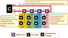
The company has overcome this problem with the development of a bridge chip that connects the controller and flash memory chips (Fig. 1), three novel techniques: a daisy chains connection including the controller and bridge chips in a ring shape; a serial communication using PAM 4; and a jitter improvement technique for eliminating a PLL circuit in the bridge chips. By using these techniques overhead of the bridge chips is reduced, and it is possible to operate a large number of flash memory chips at high speed with only a few high-speed signal lines (Fig. 2).
The ring-shape configuration of the bridge chips and the controller reduces the number of transceivers required in the bridge chip from two pairs to one pair, it achieves chip area reduction of the bridge chip. In addition, adopting PAM 4 serial communication between the controller and the daisy-chained bridge chips lowers the operating speed in the bridge chips' circuits and relaxes their required performance. A new CDR*5 that utilizes the characteristics of PAM 4 to improve jitter characteristics eliminates the need for a PLL circuit in the bridge chip, which also contributes to a smaller chip area and lower power consumption.
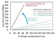
The prototype bridge chips were fabricated with 28 nm CMOS process, and results were evaluated by connecting four bridge chips and a controller in ring-shape daisy chain. This confirmed satisfactory performance of PAM 4 communication by all of the bridge chips and the controller at 25.6 Gbps, and also that it is possible to obtain a BER*6 of less than 10-12.
Moving forward, the company will continue development work toward achieving high-speed, large-capacity storage at levels not yet seen by further enhancing bridge-chip performance while reducing the chip's area and power consumption.
Notes
View at TechPowerUp Main Site
In SSDs, multiple flash memory chips are connected to a controller that manages their operation. As more flash memory chips are connected to a controller interface, operating speed degrades, so there are limits to the number of chips that can be connected. In order to increase capacity, it is necessary to increase the number of interfaces, but that results in an enormous number of high-speed signal lines connected to the controller, making it more difficult to implement the wiring on the SSD board.


The company has overcome this problem with the development of a bridge chip that connects the controller and flash memory chips (Fig. 1), three novel techniques: a daisy chains connection including the controller and bridge chips in a ring shape; a serial communication using PAM 4; and a jitter improvement technique for eliminating a PLL circuit in the bridge chips. By using these techniques overhead of the bridge chips is reduced, and it is possible to operate a large number of flash memory chips at high speed with only a few high-speed signal lines (Fig. 2).
The ring-shape configuration of the bridge chips and the controller reduces the number of transceivers required in the bridge chip from two pairs to one pair, it achieves chip area reduction of the bridge chip. In addition, adopting PAM 4 serial communication between the controller and the daisy-chained bridge chips lowers the operating speed in the bridge chips' circuits and relaxes their required performance. A new CDR*5 that utilizes the characteristics of PAM 4 to improve jitter characteristics eliminates the need for a PLL circuit in the bridge chip, which also contributes to a smaller chip area and lower power consumption.
The prototype bridge chips were fabricated with 28 nm CMOS process, and results were evaluated by connecting four bridge chips and a controller in ring-shape daisy chain. This confirmed satisfactory performance of PAM 4 communication by all of the bridge chips and the controller at 25.6 Gbps, and also that it is possible to obtain a BER*6 of less than 10-12.
Moving forward, the company will continue development work toward achieving high-speed, large-capacity storage at levels not yet seen by further enhancing bridge-chip performance while reducing the chip's area and power consumption.
Notes
- 1 Daisy chain: a connecting scheme in which multiple chips are wired together in sequence
- 2 PAM 4: 4-level Pulse Amplitude Modulation (it contains a 4-value data)
- 3 Jitter: Fluctuation in the time domain of the clock or signal waveforms
- 4 PLL: Phase Locked Loop (a circuit that generates an accurate reference signal)
- 5 CDR: Clock Data Recovery (a circuit that recovers the data and clock from the received signal)
- 6 BER: Bit Error Rate (the lower value is the better performance)
View at TechPowerUp Main Site


