• Welcome to TechPowerUp Forums, Guest! Please check out our forum guidelines for info related to our community.
  • The forums have been upgraded with support for dark mode. By default it will follow the setting on your system/browser. You may override it by scrolling to the end of the page and clicking the gears icon.

AMD Ryzen 3000 "Matisse" I/O Controller Die 12nm, Not 14nm

btarunr

Editor & Senior Moderator
Staff member
Joined
Oct 9, 2007
Messages
47,847 (7.39/day)
Location
Dublin, Ireland
System Name RBMK-1000
Processor AMD Ryzen 7 5700G
Motherboard Gigabyte B550 AORUS Elite V2
Cooling DeepCool Gammax L240 V2
Memory 2x 16GB DDR4-3200
Video Card(s) Galax RTX 4070 Ti EX
Storage Samsung 990 1TB
Display(s) BenQ 1440p 60 Hz 27-inch
Case Corsair Carbide 100R
Audio Device(s) ASUS SupremeFX S1220A
Power Supply Cooler Master MWE Gold 650W
Mouse ASUS ROG Strix Impact
Keyboard Gamdias Hermes E2
Software Windows 11 Pro
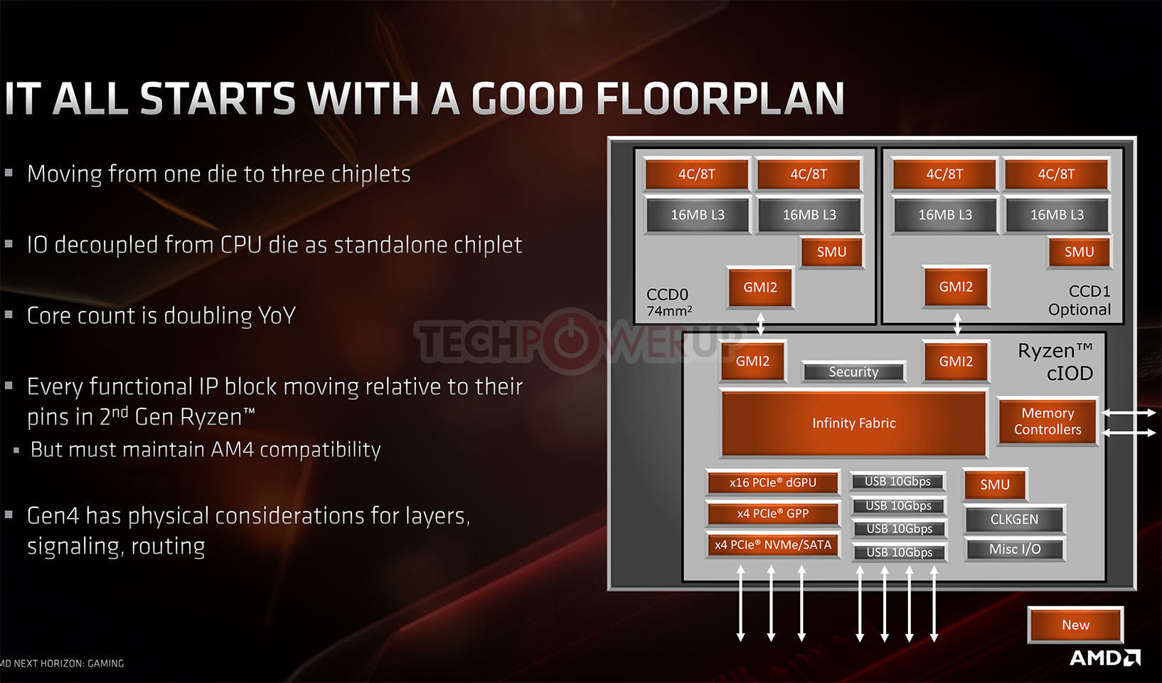
AMD Ryzen 3000 "Matisse" processors are multi-chip modules of two kinds of dies - one or two 7 nm 8-core "Zen 2" CPU chiplets, and an I/O controller die that packs the processor's dual-channel DDR4 memory controller, PCI-Express gen 4.0 root-complex, and an integrated southbridge that puts out some SoC I/O, such as two SATA 6 Gbps ports, four USB 3.1 Gen 2 ports, LPCIO (ISA), and SPI (for the UEFI BIOS ROM chip). It was earlier reported that while the Zen 2 CPU core chiplets are built on 7 nm process, the I/O controller is 14 nm. We have confirmation now that the I/O controller die is built on the more advanced 12 nm process, likely GlobalFoundries 12LP. This is the same process on which AMD builds its "Pinnacle Ridge" and "Polaris 30" chips. The 7 nm "Zen 2" CPU chiplets are made at TSMC.

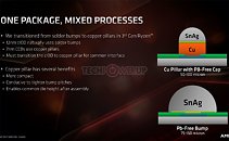
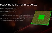
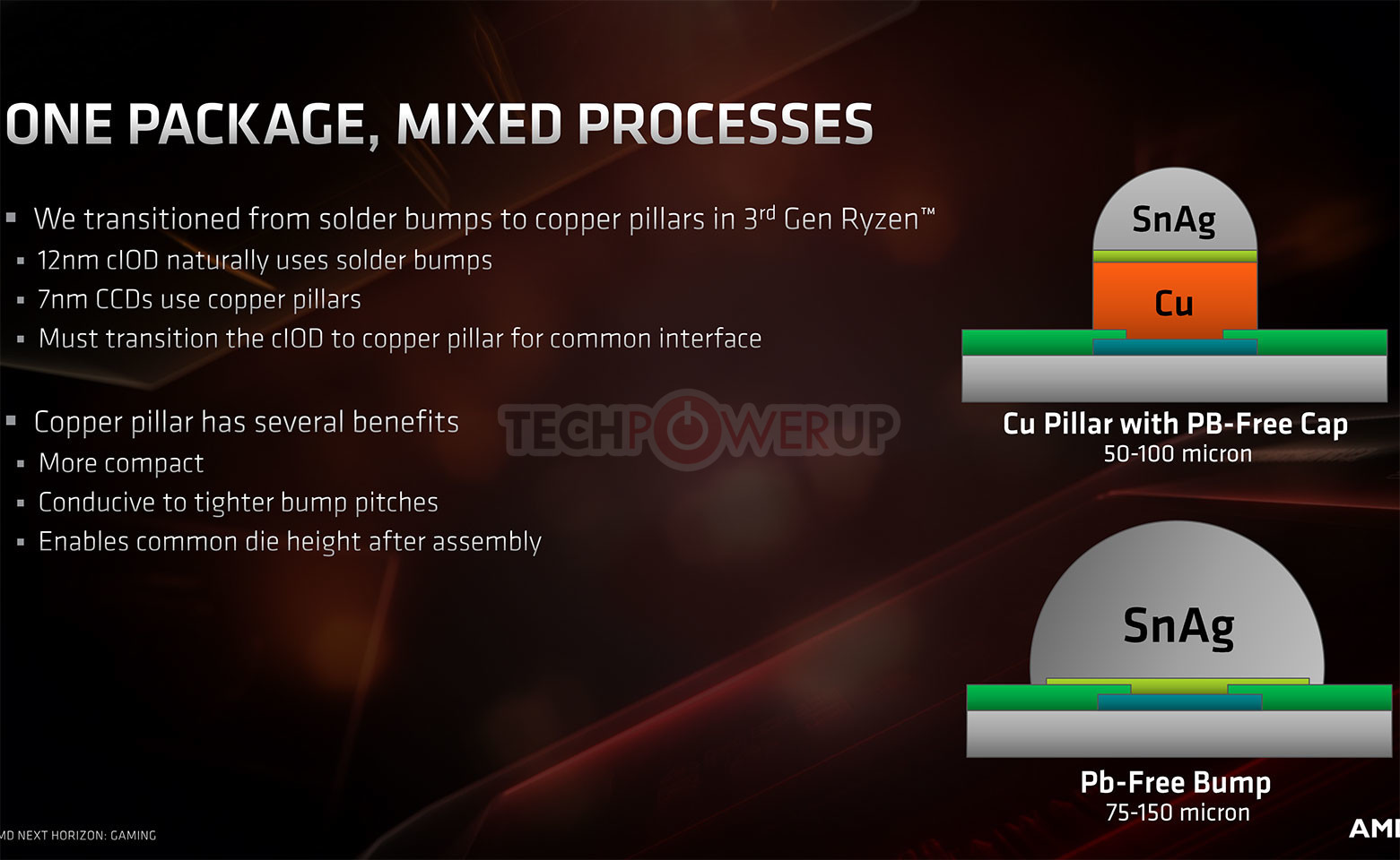
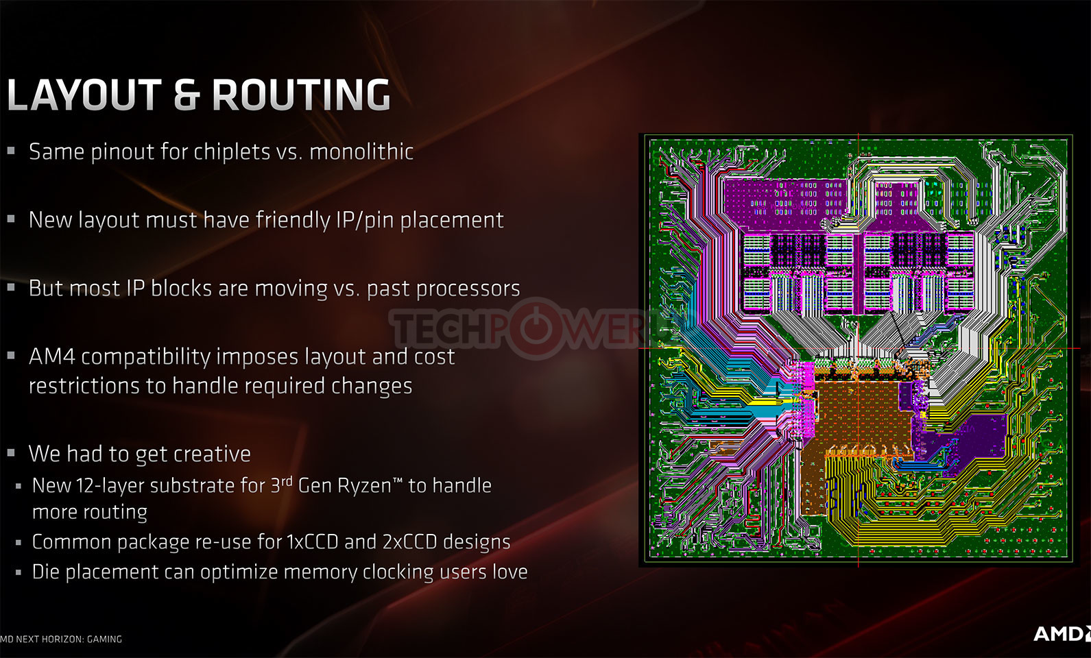
AMD also provided a fascinating technical insight to the making of the "Matisse" MCM, particularly getting three highly complex dies under the IHS of a mainstream-desktop processor package, and perfectly aligning the three for pin-compatibility with older generations of Ryzen AM4 processors that use monolithic dies, such as "Pinnacle Ridge" and "Raven Ridge." AMD innovated new copper-pillar 50µ bumps for the 8-core CPU chiplets, while leaving the I/O controller die with normal 75µ solder bumps. Unlike with its GPUs that need high-density wiring between the GPU die and HBM stacks, AMD could make do without a silicon interposer or TSVs (through-silicon-vias) to connect the three dies on "Matisse." The fiberglass substrate is now "fattened" up to 12 layers, to facilitate the inter-die wiring, as well as making sure every connection reaches the correct pin on the µPGA.


View at TechPowerUp Main Site
 
Some Reddit and Twitter posts said the I/O die is exactly the X570 chipset die , Real ?
 
This is giving me some 80s' retro style vibe

124856
 
Now I can see why 300 series chipset compatibility was such an issue.
 
Are they still connecting 4+4 cores internally via IF or is the cpu die a monolithic 8 core?
 
This is giving me some 80s' retro style vibe

View attachment 124856

This is Gerber file from the layout. You can be very creative in Gerber viewer tools with choices of colors to display different layers. :D
That is a complex layout with all the routing of differential/single ended lines many of them being impedance controller and one can also see the length matching paterns.

In other thread about x570 mainboards, there was discussions about number of layers used in mainboards. When one looks at the routing inside the processor die it is hard to image that mainboard designers can use 6 layer stackup to rout all theses signals from below the processor on only six layer PCB in mainboards.
 
Last edited:
Are they still connecting 4+4 cores internally via IF or is the cpu die a monolithic 8 core?
I think 4+4. That's what I get from the pictures.
 
Some Reddit and Twitter posts said the I/O die is exactly the X570 chipset die , Real ?

Yes, my contact in the motherboard industry agrees. They're the same die, packaged differently. The chipset version runs cooler than the iCOD version because the memory controller is power-gated (dead). AMD designed the silicon such that PCIe lanes easily convert to SATA 6G PHYs, complete with AHCI+RAID support, or even USB 3.1 gen 2. Motherboard designers have many ways of playing with this feature. Of course this makes the chipset a lot more expensive than ASMedia X470. Contact also says that the B450-successor which will come out late-2019 or early-2020 will be a new ASMedia chip with PCIe gen 4 support (and possibly Chimera-hardening). It will be as feature-rich as X470. If you want Ryzen 3000, don't need SLI/CFX support, and don't mind waiting till Xmas, I highly recommend waiting for that B450-successor chipset. You might not have to put up with the constant hum of a 40 mm fan.
 
Last edited:
You might not have to put up with the constant hum of a 40 mm fan.
Or just replace the heat sink/fan combo on the x570 Chipset, with a nice aftermarket full-copper heat sink and be done with it. Just like we did 15 years ago.
 
This tech is simply amazing !
It's like an entire motherboard has been downsized to the shape of a CPU.

In the past we had the CPU core (and that's ALL the CPU was), with a front side bus and that's it. Everything else (memory controller, I/O, signaling etc.) was done by the "north bridge", far, far away from the CPU core.
Now we're back to that topology, except that the north-bridge is 1cm away from the CORE(s), on a much, much faster interconnect than was possible before.

I can imagine future sockets of future CPUs integrating so much that the motherboard will be simply a board with slots and sockets for stuff (+ power delivery), existing only because the physical space is needed. But most if not all the electrical connections would go to the SoC.

You might not have to put up with the constant hum of a 40 mm fan.

I somehow have the feeling that that fan is PWM controlled with 0db mode.
So, it would only spin up if the X570 chip actually needs the heat removed... for example when transferring large amounts of data or using multiple USB 3.2 10gb ports.

Very likely in PCI-e 3.0 mode it wouldn't spin at all most of the time.

Guess we'll see soon enough.
 
74 mm^2 per 8 core CPU die, damn, that's tiny. Even though 7nm is not a mature process I bet AMD manages to get a lot of these out of a wafer.
 
This tech is simply amazing !
It's like an entire motherboard has been downsized to the shape of a CPU.

In the past we had the CPU core (and that's ALL the CPU was), with a front side bus and that's it. Everything else (memory controller, I/O, signaling etc.) was done by the "north bridge", far, far away from the CPU core.
Now we're back to that topology, except that the north-bridge is 1cm away from the CORE(s), on a much, much faster interconnect than was possible before.

I can imagine future sockets of future CPUs integrating so much that the motherboard will be simply a board with slots and sockets for stuff (+ power delivery), existing only because the physical space is needed. But most if not all the electrical connections would go to the SoC.


I somehow have the feeling that that fan is PWM controlled with 0db mode.
So, it would only spin up if the X570 chip actually needs the heat removed... for example when transferring large amounts of data or using multiple USB 3.2 10gb ports.

Very likely in PCI-e 3.0 mode it wouldn't spin at all most of the time.

Guess we'll see soon enough.

This is going on for many years already. Look at phones and their SOC's. All is housed inside one chip almost and it offers all posssible functionality. AMD has done it in a very clever way to maximize performance and keep the costs low. A 10W chipset is'nt the end of the world. I'm sure users are able to cool it passive and that the fan is temperature based and not fixed (as we had in the old days).

PCI-E 4.0 does'nt offer that much of a "extra" gain compared to 3.0. AMD said this in their own presentation. No need to jump to PCI-E 4.0 and put in a 4.0 capable card. It wont do much compared to PCI-E 3.0. What's more interesting is booting up the default PCI-E clocks from 100 to 120MHz for example.
 
Or just replace the heat sink/fan combo on the x570 Chipset, with a nice aftermarket full-copper heat sink and be done with it. Just like we did 15 years ago.
The only problem I see here in mainboards where the x570 chip sits behind GPU PCIE slot. :(
In that case it would be hard to use tall heatsink like we used to do 15 years ago due lengthy GPUs nowdays.

Back those days I hated these noisy small fans.
Zalmann used to offer nice after market chipset heatsinks but they were quite tall. I used to own one like this one back then: :p

Z20-4000-main.jpg
 
The only problem I see here in mainboards where the x570 chip sits behind GPU PCIE slot. :(
In that case it would be hard to use tall heatsink like we used to do 15 years ago due lengthy GPUs nowdays.

Back those days I hated these noisy small fans.
Zalmann used to offer nice after market chipset heatsinks but they were quite tall. I used to own one like this one back then: :p

View attachment 124873

Yeah, I think it should be doable with heatpipe cooler today too.
will be a bit flimsy but will be passive.
 
Yeah, I think it should be doable with heatpipe cooler today too.
will be a bit flimsy but will be passive.
Or maybe companies like EK will come up with combined water blocks to cover processor, VRMs and chipset for popular mainboards. :rolleyes:
 
It was the north bridges back in the day mobos that needed the extra cooling.

epoxep4sda_all.jpg


s-l640.jpg
 
There were also back then Nvidia nforce chipset generations that had loud fans.
 
This was still the most extreme chipset cooler ever imho.
p35p_circu2.jpg
 
IMO don't worry to much about the chipset fan, if this will be an issue - there will be an after market solution, since the popularity of X570 will be high.
Edit:
TheLostSwede
OMG this is not a cooler- this is ART!.
Edit 2:
Looks like they mad a better one later on-I miss this days, not like the lame ALU blocks :-:)
msi8.jpg
msi6.jpg

 
Last edited:
PCI-E 4.0 does'nt offer that much of a "extra" gain compared to 3.0. AMD said this in their own presentation. No need to jump to PCI-E 4.0 and put in a 4.0 capable card. It wont do much compared to PCI-E 3.0. What's more interesting is booting up the default PCI-E clocks from 100 to 120MHz for example.

That's what Intel said

IMO don't worry to much about the chipset fan, if this will be an issue - there will be an after market solution, since the popularity of X570 will be high.
Edit:
TheLostSwede
OMG this is not a cooler- this is ART!.
Edit 2:
Looks like they mad a better one later on-I miss this days, not like the lame ALU blocks :-:)
msi8.jpg
msi6.jpg


Better, most likely, but not as wacky or weird...
 
I don't really understand why do we still need an additional chipset / south bridge when the cpu has native / built-in:

the memory controller, pci-e controller and enough pci-e 4.0 lanes for a 16x vga, nvme and sata drives and usb controller for usb ports and there are still a few free pci-e lanes left for pci-e 1x slots for sound card or sata controller if needed. :confused:
 
I don't really understand why do we still need an additional chipset / south bridge when the cpu has native / built-in
Yes, it does:

- 2 SATA ports OR 4 PCI-e lanes (1 single NVMe drive), so no more SATA at all if you use one single NVMe drive)
- 2 USB 3.1
- 16 PCIe lanes for GPU
- Audio chip link.

+ 4 free PCI-e lanes which work together.

So what are you going to do with those ?
- Network ? Then you won't have any extra USBs
- USBs? Then you won't have any SATA... or network, or wifi, or anything else
- SATA? Then give up on USBs and the rest...

Obviously all these options are very bad, so you need a device that gets 4 lanes in and a whole bunch of lanes out + other ports (USB, SATA, etc.)
That's what the chipset/south bridge does... and in case of amd's X370, X470, X570... that's A LOT of stuff which it offers, even more than Intel ones.

And it works because it's extremely rare that all of the devices will communicate all at once, so the 4 lanes between CPU and SB are more than enough.
I did manage however to overload them by copying from 4 SATA SSDs to NVMe drive and from network to USB 3.1 external drives all at once. (Intentionally overloading the south bridge) But that's an extremely rare use case.
 
I don't really understand why do we still need an additional chipset / south bridge when the cpu has native / built-in:

the memory controller, pci-e controller and enough pci-e 4.0 lanes for a 16x vga, nvme and sata drives and usb controller for usb ports and there are still a few free pci-e lanes left for pci-e 1x slots for sound card or sata controller if needed. :confused:

Because the "chipset" inside the CPU doesn't offer enough connectivity within a reasonable package size. Hence why the Threadripper CPUs are so huge. This makes for much more expensive motherboards and CPU packages.
 
Back
Top