- Joined
- Oct 9, 2007
- Messages
- 47,894 (7.38/day)
- Location
- Dublin, Ireland
| System Name | RBMK-1000 |
|---|---|
| Processor | AMD Ryzen 7 5700G |
| Motherboard | Gigabyte B550 AORUS Elite V2 |
| Cooling | DeepCool Gammax L240 V2 |
| Memory | 2x 16GB DDR4-3200 |
| Video Card(s) | Galax RTX 4070 Ti EX |
| Storage | Samsung 990 1TB |
| Display(s) | BenQ 1440p 60 Hz 27-inch |
| Case | Corsair Carbide 100R |
| Audio Device(s) | ASUS SupremeFX S1220A |
| Power Supply | Cooler Master MWE Gold 650W |
| Mouse | ASUS ROG Strix Impact |
| Keyboard | Gamdias Hermes E2 |
| Software | Windows 11 Pro |
Intel's silicon fabrication technological edge over TSMC and Samsung may have buckled, but the company appears to have made big advances in chip packaging. We've known for some time about EMIB (embedded multi-die interconnect bridge), Intel's cost-effective alternative to using full-fledged interposers; and Foveros heterogenous multi-die packaging; but the company has apparently invented more forms of 3-D chip stacking, as detailed by a WikiChip Fuse report. By leveraging ODI (omni-directional interconnect), an evolutionary next-step to EMIB and Foveros, Intel is able to stack multiple chips above the fiberglass substrate, above each other; and inside indentations and cavities of the substrate.
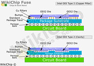
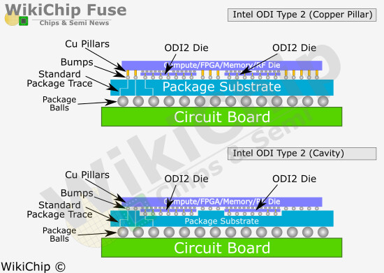
ODI consists of EMIB-like silicon dies that enable high-density wiring between two dies (think a GPU and its memory stack, or an SoC and core-logic); and copper poles that serve as extensions of the bumps of silicon dies getting to the substrate. There are two types of ODI. Type-1 refers to an interconnect running between two top dies, with the ODI die sitting between them and the substrate at the point of the inter-die connection region; while copper poles compensate for the Z-height difference. In scenarios without copper poles, chip designers can opt for substrates with cavities (regions with fewer layers), where the ODI die can be slotted in. In type-2 ODI, the interconnect die sits completely under a top die, providing high-density wiring either between two regions of the same die, or between two dies. The two types can be mixed and matched to achieve extremely complex MCMs.


View at TechPowerUp Main Site
