• Welcome to TechPowerUp Forums, Guest! Please check out our forum guidelines for info related to our community.
  • The forums have been upgraded with support for dark mode. By default it will follow the setting on your system/browser. You may override it by scrolling to the end of the page and clicking the gears icon.

NVIDIA GeForce RTX 3090 "Ampere" Alleged PCB Picture Surfaces

AleksandarK

News Editor
Staff member
Joined
Aug 19, 2017
Messages
3,205 (1.11/day)
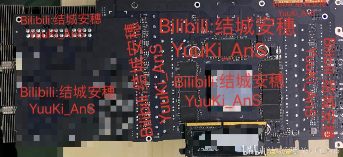
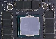
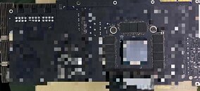
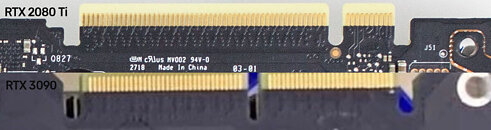
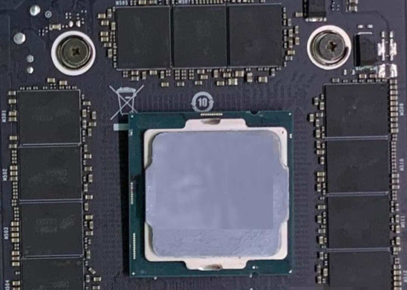
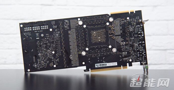
As we are getting close to September 1st, the day NVIDIA launches its upcoming GeForce RTX graphics cards based on Ampere architecture, we are getting even more leaks. Today, an alleged PCB of the NVIDIA's upcoming GeForce RTX 3090 has been pictured and posted on social media. The PCB appears to be a 3rd party design coming from one of NVIDIA's add-in board (AIB) partners - Colorful. The picture is blurred out on the most of the PCB and has Intel CPU covering the GPU die area to hide the information. There are 11 GDDR6X memory modules covering the surrounding of the GPU and being very near it. Another notable difference is the NVLink finger change, as there seems to be the new design present. Check out the screenshot of the Reddit thread and PCB pictures below:


More pictures follow:


View at TechPowerUp Main Site
 
That looks like an intel CPU stuck on a PCB

edit: okay reading first, that IS an intel CPU. wtf is the point of the pictures then?
 
Please remind me, how did it work with 5700 series.
Were there also no credible leaks until the very reveal date?
 
wtf is the point of the pictures then?

Well, you can also see that it has three 8-pin connectors. On a reference card ...
 
Sorry, I don't see it, could you elaborate?

k.png
 
This is an AIB model not FE. Memory on the back of the PCB, ie clamshell mode. CPU is hiding another ASIC. 3x8pin. Revised Nvlink. Back drill pcb. Apparently...

Exactly, we are looking at the back. This is possibly a co-processor like chip. 1GB memory modules front and back to 22GB total.
 
3 x 8-pin .........

Quite an electric heater
 
With 3X 8-PIN power connectors, this is a 500W+ card. Something wrong has happened with Ampere that they need to draw that much power to offer a generational leap over the 250-300W 2080 Ti. Yes, rumours are this is 40% faster than that card, but it draws about 40% more power. So the rumours of Nvidia going with the borked Samsung 8nm process instead of TSMC's superior 7nm+ appear true.
 
11GB or 22GB VRAM?
 
Memory in the back of the PCB? It's been a while since we've seen that on an Nvidia consumer board. 22GB of GDDR6 on a 352-bit bus?
 
96b4e89799ad033a0bfb28d0b098d4c827badb35.jpg


Here is a better image. Maybe hiding more Ram?

ooops....deleted


NVIDIA-GeForce-RTX-PCB-1200x549.jpg
 
Last edited:
Exactly, we are looking at the back. This is possibly a co-processor like chip. 1GB memory modules front and back to 22GB total.

Yeah fascinating layout, looks like the rumours of an additional co-processor could indeed be true.

Not long now either way, looks like the performance goal posts are about to move again.
 
Interesting to say the least but I still have some issues in terms of credibility...
 
Nice, and GDDR6X confirmed too.
 
This is the worst fake I've seen in a long time....

It's a newer 10th gen i3 Intel CPU.... probably using MS Paint....

Clearly the IHS is identical and even the markings on the side of the chip are identical...why would Nvidia put guide slots on the side of their new GPU when it doesn't have an INTEL socket... plus you can even see the markings of the IHS on the side where it was already mounted....lame

mate you did worse than me, read the actual text
 
With 3X 8-PIN power connectors, this is a 500W+ card. Something wrong has happened with Ampere that they need to draw that much power to offer a generational leap over the 250-300W 2080 Ti. Yes, rumours are this is 40% faster than that card, but it draws about 40% more power. So the rumours of Nvidia going with the borked Samsung 8nm process instead of TSMC's superior 7nm+ appear true.
Or this is a testing card... remember how the 2080 Ti PCBs were leaked? Same story. It's a testing card.
 
Back
Top