• Welcome to TechPowerUp Forums, Guest! Please check out our forum guidelines for info related to our community.

NVIDIA GeForce RTX 3090 Ampere Bare PCB Pictured

btarunr

Editor & Senior Moderator
Staff member
Joined
Oct 9, 2007
Messages
47,895 (7.38/day)
Location
Dublin, Ireland
System Name RBMK-1000
Processor AMD Ryzen 7 5700G
Motherboard Gigabyte B550 AORUS Elite V2
Cooling DeepCool Gammax L240 V2
Memory 2x 16GB DDR4-3200
Video Card(s) Galax RTX 4070 Ti EX
Storage Samsung 990 1TB
Display(s) BenQ 1440p 60 Hz 27-inch
Case Corsair Carbide 100R
Audio Device(s) ASUS SupremeFX S1220A
Power Supply Cooler Master MWE Gold 650W
Mouse ASUS ROG Strix Impact
Keyboard Gamdias Hermes E2
Software Windows 11 Pro
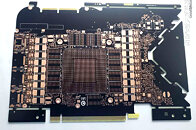
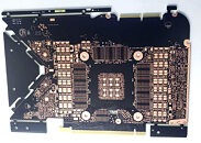
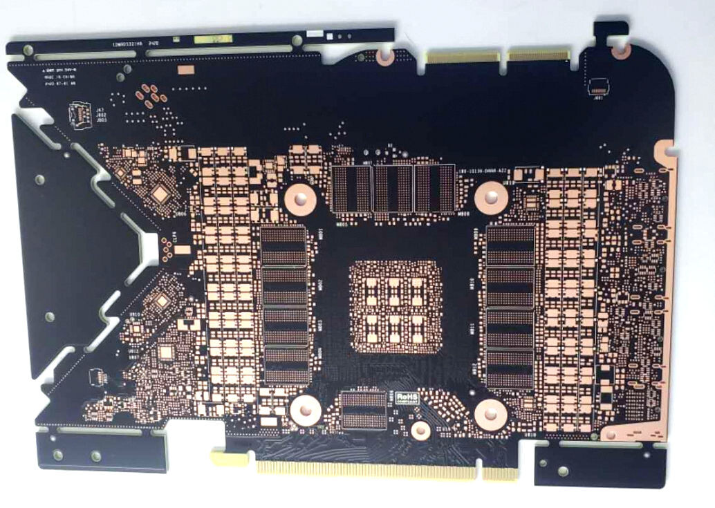
Here are some of the clearest pictures of an NVIDIA GeForce RTX 3090 "Ampere" Founders Edition PCB, albeit bare (components not yet placed). The PCB goes in this form to another production line, where a PCB placer machine with reels of components places them along both sides. We can still make out quite a few things. To beign with, there are six high current traces near where the 12-pin Molex MicroFit power connector goes in.

NVIDIA seems to have utilized both sides of the PCB effectively. The card features traces for a mammoth 20-phase VRM. The obverse side has the chokes and DrMOS, the reverse side has the capacitors. Twelve memory pads for the 384-bit wide GDDR6X memory interface surround the GPU pad. There are pads for four display output connectors, which could be a mixture of DisplayPort, HDMI, or even USB-C VirtualLink. The PCB still has its spacers on, which will be cut out after component placement, after which the PCB heads for testing and product assembly. NVIDIA is expected to announce the GeForce RTX 3090 Ampere at an online event later today.


View at TechPowerUp Main Site
 
Very short PCB. That gigantic cooler makes the card long.
 
well finally we have undeniable proof that this taversal coprocessor stuff was nonsense...
also the amount of phases the RTX 3090 would have was allready calculated by Igor from igorslab.de in June (!)

only things missing now are the exact structure of the cooler and perfomance numbers. Gimme!
 
Very short PCB. That gigantic cooler makes the card long.

Very nice design. Before, you always got huge empty pcbs for big cooler cards, this way the pcb is only the size it needs to be, letting the radiator breathe better and do a better job. I don't know how big is the added complexity of manufacturing this, but it's definitely a step in the good direction.
I mean, GPU TDPs are goind up anyway, it would be better if the cooling design allowed for better cooling capacity in the future. CPU coolers have it way easier.
 
I wonder if there will be a RTX 3090 Ti
 
I wonder if there will be a RTX 3090 Ti
You mean wearing that exact name? That's not sure, it seems Nvidia are trying to clean up their naming scheme a bit. But if you mean a stronger Ampere card than the 3090, there's a high chance for that.
 
i think 3090 is titan but maybe im wrong but nevertheless i think there will be 3080 ti to fill the space in shader units between 3080 and 3090
 
i think 3090 is titan but maybe im wrong but nevertheless i think there will be 3080 ti to fill the space in shader units between 3080 and 3090

I think there's a 48GB full-fat GA102 Titan coming later
 
You mean wearing that exact name? That's not sure, it seems Nvidia are trying to clean up their naming scheme a bit. But if you mean a stronger Ampere card than the 3090, there's a high chance for that.

Of course there will be. For all the enthusiasts that spent four digits for a 3090 now and don't care for spending another 2k a couple of months later just to keep having the biggest... I mean fastest GPU.

Anyways, I like the size of that PCB. Is it true, that all tiers will use the same PCB like with the 16xx cards? I will probably get a 3070 or maybe the AMD equivalent after RDNA2 is released. With watercooling attached, something this small could be a great little addition to my ITX system.
 
Ampere, worst kept secret ever.
 
Ampere, worst kept secret ever.
Its called marketing. Do you really think that most of these leaks are involuntary? Its all part of the release process.
 
Very short PCB. That gigantic cooler makes the card long.
There's still a possibility of a separate PCB containing some of the stuff (I don't see any mounts for power supply in the pics above), there's also this:
09_nvidia_geforce_rtx_3080_z_rdzeniem_ampere_ga102_i_gddr6x_1_b.jpg


Until I see the whole card I'll wait with my opinions about how small the card is. :)
 
To beign with, there are six high current traces near where the 12-pin Molex MicroFit power connector goes in.
The 12-pin microfit connector area is indeed interesting.

There are pads for four display output connectors, which could be a mixture of DisplayPort, HDMI, or even USB-C VirtualLink.
They are double stacked pads.
 
What is interesting is that the 12-pin PCIe Molex connector capable of 600+ gazillion watts only has 4 receptacle through holes on the PCB (2 ground, 2 +12V).
 
Hmm about 20 VRM's stacked closely to its other.
Next thing we need to know this is : How many layers and thickness of the PCB.

A large number of VRM's this translates that the GPU has the ability to turn off engines that the software can not use them.
Its like an active power saving mechanism.
 
Last edited:
Well shit, that's one sexy PCB.
 
What is interesting is that the 12-pin PCIe Molex connector capable of 600+ gazillion watts only has 4 receptacle through holes on the PCB (2 ground, 2 +12V).
I count six, which I would guess is four for +12V and two for ground.

They are double stacked pads.

Uhm, only one allows for either HDMI or DP, the other three are DP, although there is something going on with the top most port, as there's space for a chip underneath the connector, which is highly unusual.
However, none of them are double stacked, if you compare with this. It also makes it clear that the 3090 doesn't have a USB-C port for VirtualLink.

NVIDIA-GeForce-GTX-2080-1180-PCB-1-1000x490.jpg


@btarunr the PCB has space for 24 memory ICs, not 12, as there are 12 pads on each side.

It's interesting to see a graphics card with more power phases than most high-end motherboards. That must be one power hungry chip.

Next thing we need to know this is : How many layers and thickness of the PCB.
Sadly it's a bit too blurry to see, but it seems to be a 12 layer PCB if you look at the rear picture of the PCB and up top there's a yellow-ish square where I'm guessing the PCB layer number is present and it looks like a 12 to me.
 
4x DP with the option of swapping the bottom one for a single HDMI port.

If they can cram the GA102 on ~205mm, a sub 170mm card should be trivial for GA104...
 
I count six, which I would guess is four for +12V and two for ground.

The two smaller ones are reinforcement pins for a partial metal plate.
 
There's still a possibility of a separate PCB containing some of the stuff (I don't see any mounts for power supply in the pics above), there's also this:
09_nvidia_geforce_rtx_3080_z_rdzeniem_ampere_ga102_i_gddr6x_1_b.jpg


Until I see the whole card I'll wait with my opinions about how small the card is. :)
The picture is just some fanfiction. What would possibly be in the additional pcb anyway, when you can clearly see that everything necessary is already in the news articles pcb picture.
What is interesting is that the 12-pin PCIe Molex connector capable of 600+ gazillion watts only has 4 receptacle through holes on the PCB (2 ground, 2 +12V).
300 Watts before it will start to heat up in an unhealthy manner. The PCB mounting points can carry that no problem, the thin wires and connection points inside the plug & receptacle are the problem areas. It’ll be interesting to see what figure nvidia will tout in the evenings presentation.
 
You still know very little about how it performs, hours before its release.
The hype machinery has to start somewhere. What's interesting about all of it is, I can't remember when has this last happened with an Nvidia release. The amount of" leaks" rivals some of the biggest Amd's hype trains.
Which is weird because there's not much known about RDNA2, and I'm guessing that card is launching very soon as well.
 
Layout routing of this board must be real fun :). Placing of big VRM so close to sensitive high-speed traces is SI nightmare :)
 
Which is weird because there's not much known about RDNA2, and I'm guessing that card is launching very soon as well.
Sometime in November, according to that weird twitter dude that was spot on on number of CUs in 3xxx lineup.
 
Back
Top